482 1st passive Sigma Delta ADC
482 : 1st passive Sigma Delta ADC

- Author: Joerg Vollrath
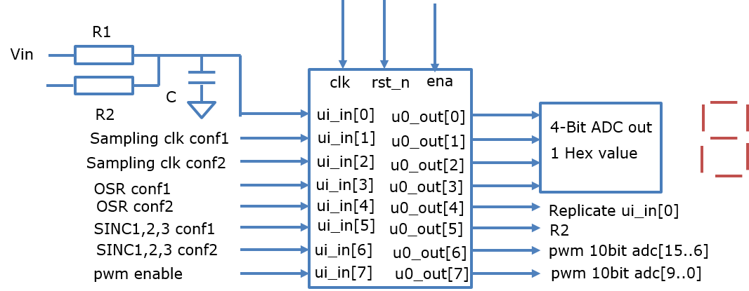
- Description: External R1 and R2 and C2 realize a ADC
- GitHub repository
- Open in 3D viewer
- Clock: 1000 Hz
How it works
A 1st order passive sigma delta modulator can be realized by attaching R1, R2 and C to a digital input. Further information is found here: https://personalpages.hs-kempten.de/~vollratj/InEl/SigmaDelta_ADC_real.html
A high level simulator: https://personalpages.hs-kempten.de/~vollratj/InEl/SigmaDelta.html
How to test
Add the RC network and apply a DC voltage at the input in0 and out5. Select sampling, oversamplingrate and filter in1..6. The 4 output lines 0..3 should give a 4-Bit value. The out6,7 give a pwm signal changing with the input voltage.
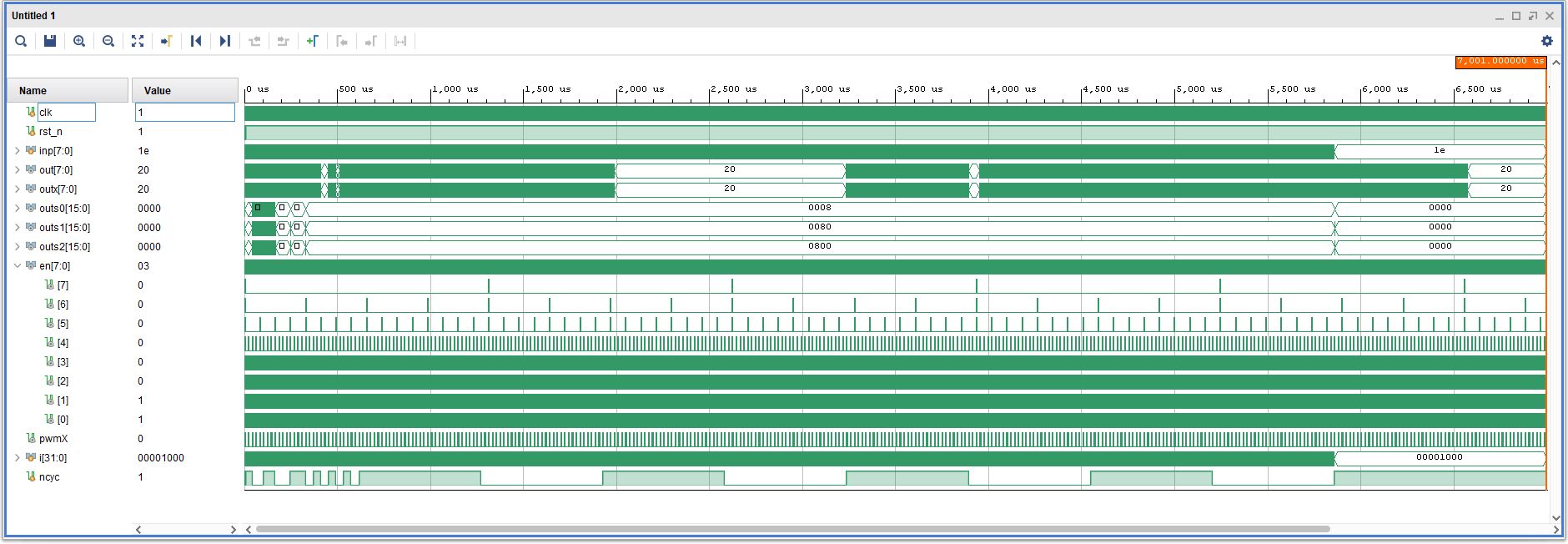
All subcircuits were tested in one testfile tb_sigdel do be able to observe all signals.
BASYS3 board measurements
22k resistors were used with 100 and 560 pF capacitances.
The signals at the capacitor and the digital signal inx were measured with an Electronic Explorer board.
Measurement showed a missing enable signal for inx sampling.
The table shows valid configuration options.
| inp[6] | inp[5] | inp[4] | inp[3] | inp[2] | inp[1] | Cint | fCLK = 50MHz | T = 20ns | OSR | Ldmax | Bits |
|---|---|---|---|---|---|---|---|---|---|---|---|
| 0 | 1 | 0 | 0 | 0 | 0 | 100 pF | SINC1 fsCLK | 40 ns | 256 | LD7 | 8 |
| 0 | 1 | 0 | 0 | 0 | 1 | SINC1 fsCLK | 160 ns | 64 | 6 | ||
| 0 | 1 | 0 | 1 | 0 | 0 | 100 pF | SINC1 fsCLK | 40 ns | 1024 | LD9 | 10 |
| 0 | 1 | 0 | 1 | 0 | 1 | SINC1 fsCLK | 160 ns | 256 | 8 | ||
| 0 | 1 | 0 | 1 | 1 | 0 | SINC1 fsCLK | 640 ns | 64 | 6 | ||
| 0 | 1 | 1 | 0 | 0 | 0 | SINC1 fsCLK | 40 ns | 4096 | 12 | ||
| 0 | 1 | 1 | 0 | 0 | 1 | SINC1 fsCLK | 160 ns | 1024 | 10 | ||
| 0 | 1 | 1 | 0 | 1 | 0 | 560 pF | SINC1 fsCLK | 640 ns | 256 | 8 ok | |
| 0 | 1 | 1 | 0 | 1 | 1 | 560 pF | SINC1 fsCLK | 2560 ns | 64 | LD5 | 6 ok |
| 0 | 1 | 1 | 1 | 0 | 0 | SINC1 fsCLK | 40 ns | 16384 | 14 | ||
| 0 | 1 | 1 | 1 | 0 | 1 | 560 pF | SINC1 fsCLK | 160 ns | 4096 | 12 ok | |
| 0 | 1 | 1 | 1 | 1 | 0 | 560 pF | SINC1 fsCLK | 640 ns | 1024 | 10 ok | |
| 0 | 1 | 1 | 1 | 1 | 1 | 560 pF | SINC1 fsCLK | 256 0ns | 256 | 8 ok | |
| 1 | 0 | 0 | 0 | 0 | 1 | SINC2 fsCLK | 64 | 12 | |||
| 1 | 0 | 0 | 0 | 1 | 0 | SINC2 fsCLK | 16 | 8 | |||
| 1 | 0 | 0 | 1 | 1 | 0 | SINC2 fsCLK | 64 | 12 | |||
| 1 | 0 | 0 | 1 | 1 | 1 | 560 pF | SINC2 fsCLK | 16 | LD7 | 8 | |
| 1 | 0 | 1 | 0 | 1 | 1 | 560 pF | SINC2 fsCLK | 64 | LD11 | 12 | |
| 1 | 1 | 0 | 0 | 1 | 0 | SINC3 fsCLK | 16 | 12 | |||
| 1 | 1 | 0 | 0 | 1 | 1 | 560 pF | SINC3 fsCLK | 4 | LD5 | 6 | |
| 1 | 1 | 0 | 1 | 1 | 1 | 560 pF | SINC3 fsCLK | 16 | LD11 | 12 |
A better configuration scheme should be chosen in the next design.<br> Higher fsCLK have lower capacitance.
A better multiplexing to the 4 Bit output with a case statement was done at the FPGA and the routing of out[3:0] done to led[3:0].
![Oscilloscope picture BASYS3 FPGA not(inx) (blue) and inp[0] (orange)](https://index.tinytapeout.com/tt06/tt_um_jv_sigdel/docs/TTsigdelOsci.jpg)
Summary
It is possible with this circuit to look at the influence of R, C and oversampling on the accuracy of a 1st order sigma delta ADC.
Bad R,C values can cause non linearities or signal limitation to VDD and ground.
The order of the SINC filter can lead to less resolution (SNR) than expected.
The order of the SINC filter should be at least one more than the sigma delta modulator.
The pwm signal has 10 bits and can be used for more precise output values.
References
Martin Knauer, Jörg Vollrath, 'Implementation and Testing of a FPGA Based Sigma Delta Analog to Digital Converter', 58. MPC Workshop, Reutlingen July 2017
IO
| # | Input | Output | Bidirectional |
|---|---|---|---|
| 0 | Input voltage input voltage R1, uo5 R2, C attached | ADC 0 LSB | |
| 1 | Sampling clock conf1 | ADC 1 | |
| 2 | Sampling clock conf2 | ADC 2 | |
| 3 | OSR conf1 | ADC 3 MSB | |
| 4 | OSR conf2 | replicate ui0 | |
| 5 | SINC1,2,3 conf1 | invert ui0 R2 | |
| 6 | SINC1,2,3 conf2 | pwm upper | |
| 7 | pwm output enable | pwm lower |