Getting started with the Tiny Tapeout Hackaday GF0p2 chip breakout
If you’ve got your hands on a GF0p2 chip breakout card, this quickstart guide will get you going and cover the following:
- overview and bringup
- interaction via microcontroller
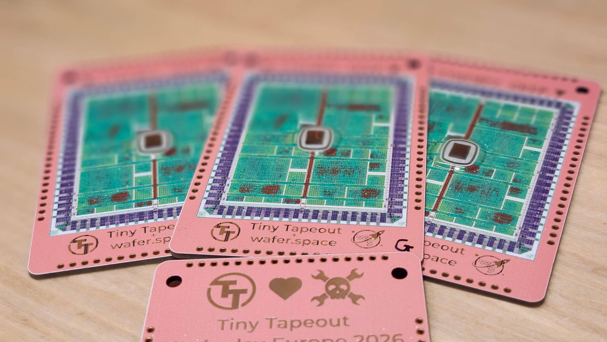
A couple of Hackaday 2026 breakout PCBs laid out on a table
Please note that you will need a microcontroller (Arduino/Pico/ESP32) to interact with the chip itself, as you’ll need to interact with the mux onboard in order to select one of 52 designs onboard.
We only had an ~80% yield of boards with all pads successfully bonded, so there is a possibility that your board may not be fully functional. If you are running into any issues, this is a possible cause. We will explain how to test whether your board is functional later in the guide.
There are two chip variants bonded to the breakout - TTP2 and TTPG. TTP2 only has a single power rail, and all
power pins should be tied together to a supply outputting 3.3V to 5V. TTPG uses separate rails for VIO and Vcore -
VIO in this case can be 3.3V or 5V, but Vcore must be 3.3V. If using different supplies for TTPG, then they must
be ramped up/down together.
Determining which variant you have will require you to bring up the chip at 3.3V first and read the onboard chip ROM or
checking if VDD Core and VDD IO are shorted - if so, then you have a TTP2 variant.
Overview
The breakout card has one of our TTGF0p2 dies wirebonded onto it - the chip contains 52 unique designs, and was manufactured using GlobalFoundries’ 180nm process. The designs onboard are fully open source, and you can learn about them all by reading our datasheet or by simply scrolling through the table of projects on the chips’ homepage.
There is a varied selection of projects on this chip: RISC-V and custom ISA processors, visual VGA creations, playable games and PLA/FPGA fabrics.
Projects have access to 10 input pins, 8 output pins and 8 bi-directional pins to interface with the outside world. The pins which the project uses should be documented in their individual datasheets. Though lacking from this breakout card, projects may also use PMOD expansion cards (which would typically be connected via some headers) in order to access additional memory (PSRAM), draw to a screen via VGA, or connect a gamepad controller.
PMODs are available from our store, or you can manufacture your own if you follow the Digilent PMOD specification. Be sure to check out our pinout specs page too!
Pinout Diagram
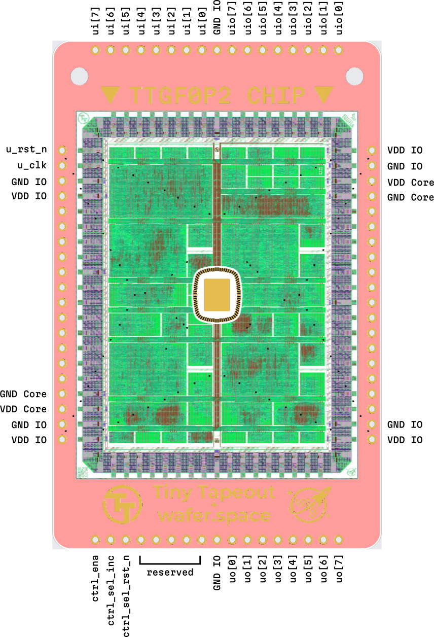
Multiplexer Crash Course
The Tiny Tapeout multiplexer distributes a single set of user IOs to multiple user designs. It forms the foundation on which multiple designs can co-exist on the same chip, enabling a low-cost MPW shuttle.
It provides the following:
- 10 dedicated inputs (shown as
ui, alongside the dedicatedclkandrst_npins) - 8 dedicated outputs (shown as
uo) - 8 bidirectional outputs (shown as
uio)
In Verilog, a single bit of a wider bus is indexed similarly to an element of an array in a programming language. This is
to say that signal ui[3] is the 4th bit of the ui bus.
It is formed of 3 distinct units:
- The controller - used to set the address of the active design
- The spine - a chip-tall buss that connects the controller with all the mux units
- Mux units - connects the spine to individual user designs
We are mostly interested in the controller. It contains 3 input lines.
| Input | Description |
|---|---|
ctrl_ena |
Sent as-is (buffered) to the downstream mux units |
ctrl_sel_rst_n |
Resets the internal address counter to 0 (active low) |
ctrl_sel_inc |
Increments the internal address counter by 1 on the rising edge |
To select a design at address 12, you need to pulse ctrl_sel_rst_n low, and then pulse ctrl_sel_inc 12 times.

Mux signals for activating the design at address 12
Explore this process with this interactive simulator below. Press the play button and then click on the INC and RST_N
buttons. Notice how the counter goes up if you keep pressing INC? This is the basic idea behind selecting a project.
Trouble viewing the simulation? Check it out on Wokwi.
Power
VDD IO and VDD Core must not exceed 3.3V. These can be shorted together on the TTPG variants.
Analog I/O
This chip does not support any analog projects.
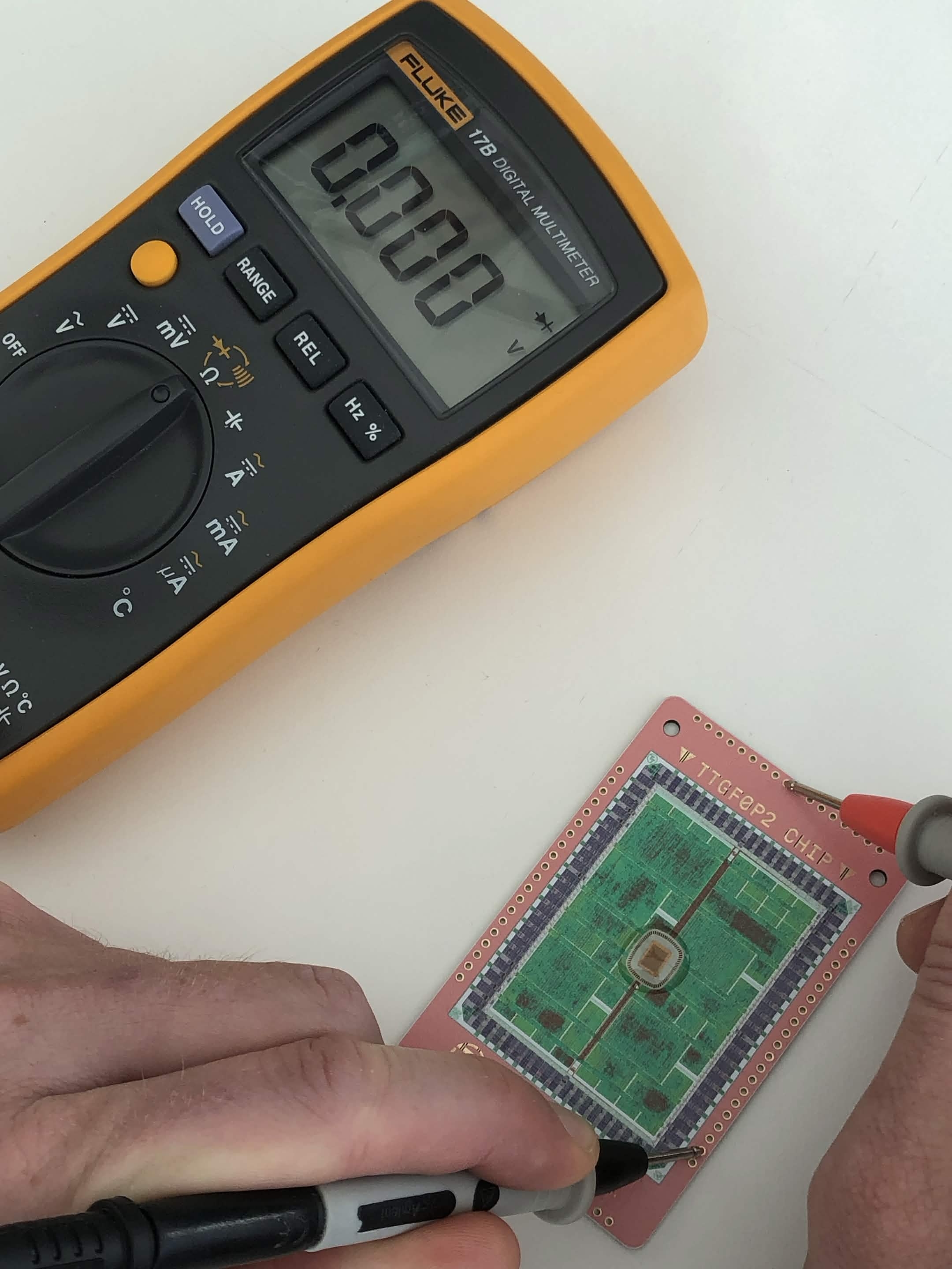
Is the chip alive?
You will require a multimeter for this section. Turn it to the diode checker mode, place the positive probe on a ground pad and observe the following:
- ~0.6V on any I/O pad
- ~0.4V on a power rail
- 0V on a ground pin
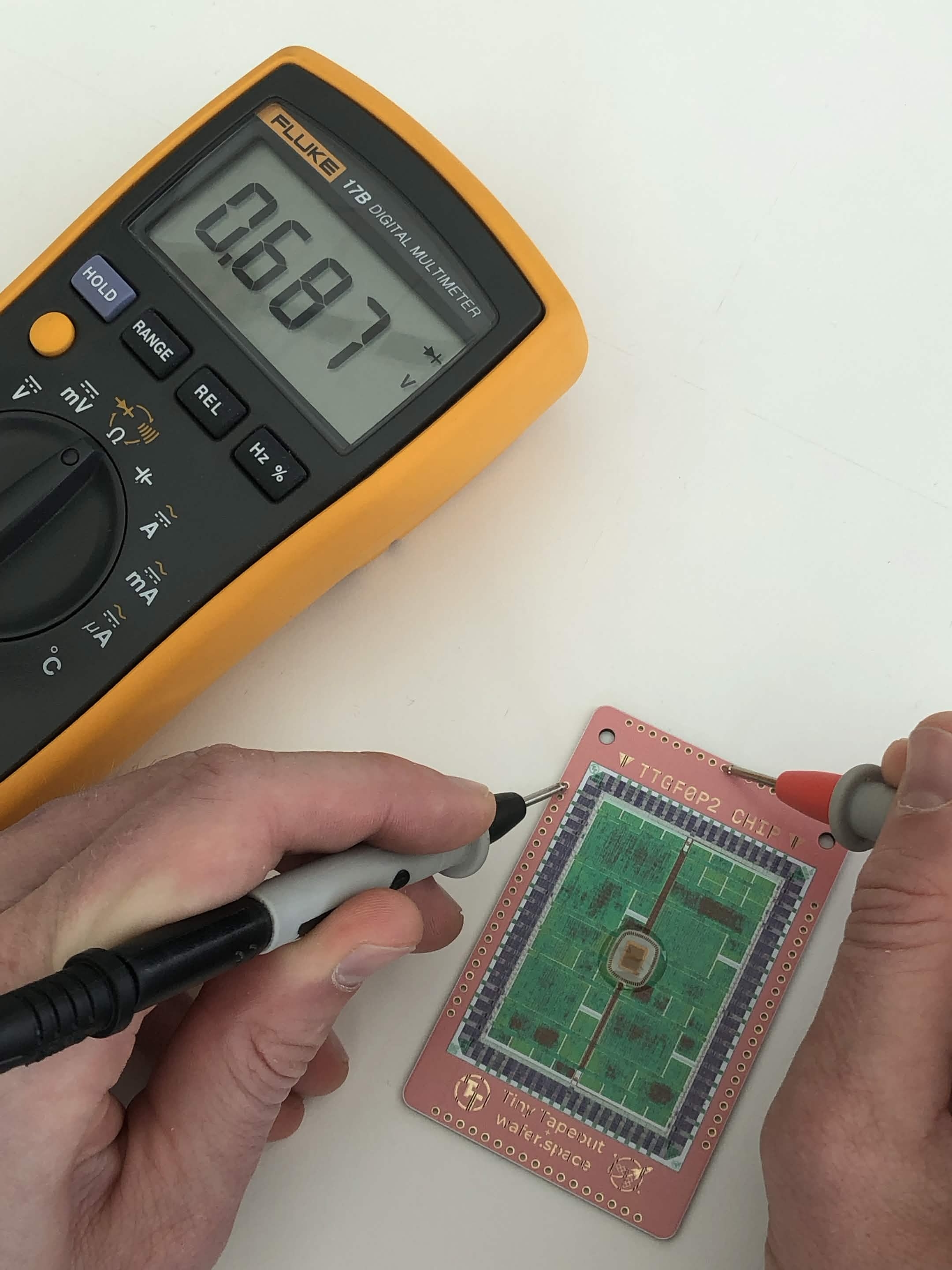
Testing the `u_rst_n` pin
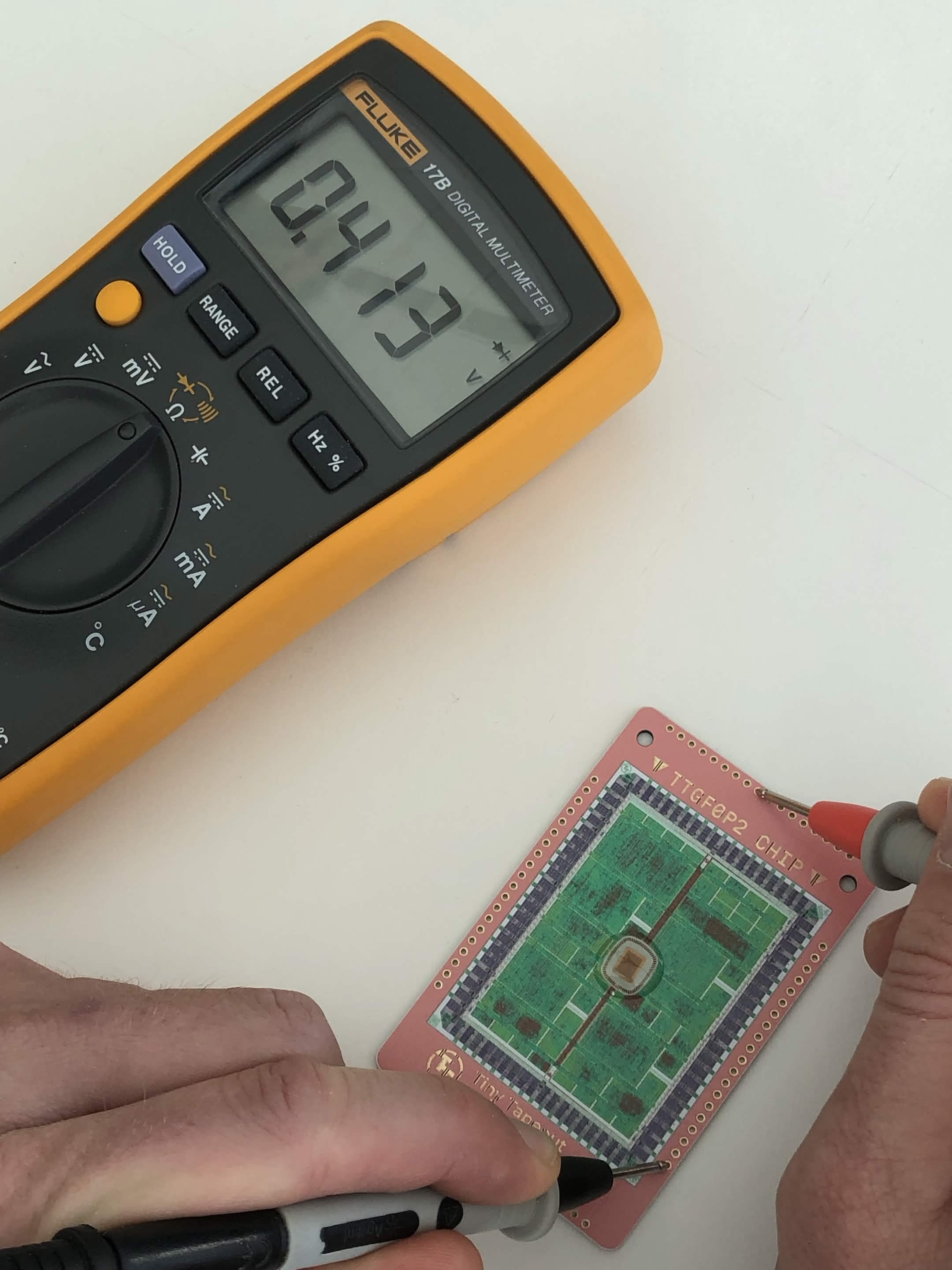
Testing VDD IO
Testing GND IO
You will have to check every pin to ensure full functionality. As mentioned before, there was an 80% success rate with the bonding, so some pins may not be connected fully.
Bring-up
We will bring-up the chip and verify that it is working by reading the on-board chip ROM.
The chip ROM contains metadata about this chip: shuttle name, git commit hash, chip descriptor, a magic value and a CRC32 of the ROM contents.
Microcontroller Firmware
Before we power on the chip, we should prepare the firmware for our microcontroller so that we can correctly initialise and control the chip. We are aiming to read the chip ROM, this means that we must:
- Select design address 0
- Set
u_rst_nhigh - Read the ROM data via
uo - Toggle the clock via the
clkpin - Repeat the above two steps until all the data has been read
It may help to familiarise yourself with an example project. Below is a Raspberry Pi Pico project which outputs the
correct control signals to select a project at address 42. Feel free to modify and experiment with the design, and
adapt it to your usecase. The function ctrl_select_design under ctrl.c is of particular interest.
Trouble viewing the simulation? Check it out on Wokwi.
Pseudocode for selecting the ROM and reading data:
char[] data;
gpio_put(CTRL_SEL_RST_N, HIGH);
gpio_put(CTRL_SEL_INC, LOW);
gpio_put(CTRL_SEL_RST_N, LOW);
gpio_put(CTRL_SEL_RST_N, HIGH);
gpio_put(CTRL_ENA, LOW);

gpio_put(U_RST_N, LOW);
gpio_put(CTRL_ENA, HIGH);

for (int i = 0; i < 256; i++) {
    data.append(gpio_read(uo));
    gpio_toggle(U_CLK);
}
Wiring
Connect the following pins to your microcontroller of choice:
- Power
- Ground
- Control signals
ctrl_enactrl_sel_incctrl_sel_rst_n
- Design interface signals
u_clku_rst_nuo[0]through touo[7]ui[0]through toui[7]uio[0]through touio[7]
If you are interested in a particular project and don’t particularly feel like wiring everything up, then have a look at the project’s pinout table - some may use less pins than provided by the chip.
Power On
Once flashed and powered on, you should see some information being printed to the terminal.
TTP2 variants
shuttle=ttgf0p2
repo=TinyTapeout/tinytapeout-gf-0p2
commit=7416232b
TTPG variants
shuttle=ttgf0p2
repo=TinyTapeout/tinytapeout-gf-0p2
commit=ff701baa
Selecting Projects
Selecting another project simple - issue a reset signal to the mux controller and pulse ctrl_sel_inc as many times
as desired! Have a browse through the project list for this shuttle and pick something that seems
interesting to you.
Some projects may require additional external hardware. This should be noted in their project’s datasheet.
Now what?
Experiment, explore and hack away! Pick a different project, try to see how it works by looking at their GitHub repo, or try and break it by feeding it weird inputs - the chip is yours to do as you please. If you do find something interesting, come tell us on discord or tag us on social media.
We hope that this inspires you to come do a tapeout of your own. We do frequent shuttles, and the community is more than willing to help out if you run into any issues.
Feedback
Do you have any feedback or suggestions? Did you run into any issues? Please let us know via our discord. If it relates to the content of this page, why not open an issue on github?