129 M0: A 16-bit SUBLEQ Microprocessor
129 : M0: A 16-bit SUBLEQ Microprocessor
- Author: William Moyes
- Description: A capable but slow microprocessor that fits in a very tight space
- GitHub repository
- Open in 3D viewer
- Clock: 12500 Hz
How it works
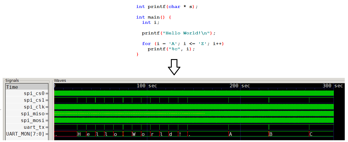
The M0 is a 16-bit, bit serial microprocessor based upon the SUBLEQ architecture. The only external devices needed for operation are a SPI RAM, SPI ROM, and clock source. The entire ROM and RAM are available for user code. All registers and logic are contained within the M0 itself. A transmit UART is included for serial output. The M0 interoperates with Oleg Mazonka's HSQ C-compiler for SUBLEQ. See https://github.com/moyesw/TT02-M0/blob/main/README.md for full details on the M0.
How to test
Easy check #1 without RAM/ROM chips- Assert Reset High (input1). Hold spi_miso low (input2). Apply a slow clock to both CLK (input0) and DBG_in (input7). Bring Reset Low. Examine the inverted clock output on output7 (DBG_OUT), and compare to clk on in0 to determine io scan chain quality. Examine spi_clk on out3. There should be 40 spi clock pulses at half the clk input frequency, followed by a 2 spi clock gap where no pulses are present.
Easy check #2 without RAM/ROM chips- Assert Reset high (input2). Hold spi_miso low. Apply a clock to CLK (input0). Bring Reset Low. Allow the M0 to reach steady state (504 clock cycles from reset). Observe the UART transmits 0xFF every 504 input clock cycles on output4. Observe that the CS0 and CS1 are accessed in the pattern: CS1, CS1, CS0, CS1, CS1, CS0. Observe that the CS0+1 and the spi_mosi pin encodes the following repeating SPI access pattern: CS1:Rd(03):Addr(FFFE), CS1:Rd(03):Addr(FFFE), CS0:Rd(03):Addr(0000), CS1:Rd(03):Addr(FFFE), CS1:Wr(02):Addr(FFFE), CS0:Rd(03):Addr(8000). Note Each access will be accompanied by 16/17 bits of data movement.
Running code with RAM/ROM chips- Connect a programmed SPI ROM to CS1, and a SPI RAM to CS0. Assert Reset. Power up the ASIC and provide a clock. Lower Reset, and observe execution. The program's serial output will appear on output pin 4 at a baud rate that is one half the input clock frequency. See https://github.com/moyesw/TT02-M0/blob/main/README.md for information on external connections, ROM and RAM data formats, instruction set, and compiler usage.
External hardware
A SPI ROM and RAM for user code
IO
| # | Input | Output |
|---|---|---|
| 0 | clk | spi_cs0 |
| 1 | rst | spi_cs1 |
| 2 | spi_miso | spi_clk |
| 3 | spi_mosi | |
| 4 | uart_tx | |
| 5 | ||
| 6 | ||
| 7 | dbg_in | dbg_out |