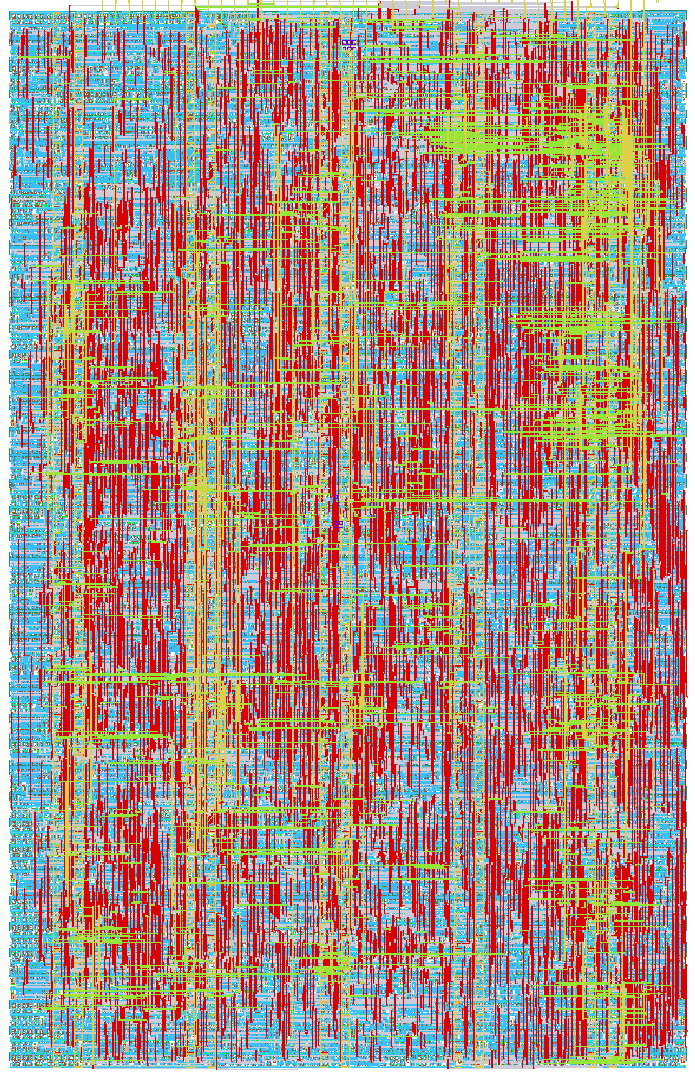
75 PWM_SPI
75 : PWM_SPI

- Author: HES SO
- Description: A PWM module controllable from an spi interface.
- GitHub repository
- Open in 3D viewer
- Clock: 50000000 Hz
How it works
PWM is a technique used to output analog results with digital means.
A digital control is used to generate digital signals that can have variable duty cycle.
The goal is to adjust the output pulse width in order to regulate the average output voltage.
Our chip is a pwm module that is controlled over an SPI interface.
SPI Command Set
These command values are sent over SPI to control the PWM peripheral:
| Command (8-bit) | Operation |
|---|---|
8'd1 |
Write Compare Value (CV) |
8'd2 |
Write Prescaler value |
8'd3 |
Write Duty Cycle 1 |
8'd4 |
Write Duty Cycle 2 |
8'd5 |
Write Duty Cycle 3 |
8'd6 |
Disable PWM output |
8'd7 |
Enable PWM output |
For operations other than ENABLE_PWM and DISABLE_PWM, the SPI command must be followed by four data bytes. These bytes represent the value to be written into the selected register (e.g., Compare Value, Prescaler, or Duty Cycle). The data is transmitted least significant byte (LSB) first, so the first byte on the SPI bus corresponds to bits [7:0] of the value, the second byte to bits [15:8], and so on, up to the most significant byte.
The SPI slave has a clock polarity of zero and clock phase of zero, CPOL=0 and CPHA=0.
Override pins are present to test the functionality of the PWM module without having to use the SPI. When driven high, the pins set the counter value, prescaler, duty cycles, and enable signal of the PWM directly to a preset value. When all override pins are driven the output signal should be 10kHz 50% duty cycle on all 3 PWM output pins when ran at 25MHz.
There are two input pins that set the output of a uio output pin to 0, 1, and Z. This is just to test functionality of tristating in tinytapeout.
How to test
Program counter value, and duty cycle registers over SPI by sending the proper command byte followed by 4 bytes to set the value of the register. Then send the enable pwm command byte to start the SPI. Outputs 3 to 7 indicate that the registers value is non zero. Bidirectional output 0 shows if the enable register is non zero. Or use the override pins present on the ui_in to test just the PWM.
External hardware
SPI master device and something to view the PWM signal with.
IO
| # | Input | Output | Bidirectional |
|---|---|---|---|
| 0 | Sets Value of uio_out0 | pwm_0 | EN_nonZero |
| 1 | High Z on uio_out0 - 1 for Z | pwm_1 | |
| 2 | CV_override | pwm_2 | |
| 3 | PS_override | CV_nonZero | High Z test Pin |
| 4 | DC1_override | PS_nonZero | spi_clk |
| 5 | DC2_override | DC1_nonZero | miso |
| 6 | DC3_override | DC2_nonZero | mosi |
| 7 | EN_override | DC3_nonZero | cs_n |