Creating Silicon Art
This guide shows you how to add silicon art — a decorative doodle, logo, or message — to your Tiny Tapeout project. When the chip is manufactured, your artwork appears as metal shapes on the die, visible under a microscope.
You do not need to understand the full ASIC flow to follow this guide. If you already have a working Tiny Tapeout repository, you can add art in a few steps.
What you’ll do
At a high level, silicon art works like placing a pre-drawn sticker on your chip layout:
- Create (or obtain) two layout files: GDS and LEF
- Put them in your repository
- Tell the build system where to place them (config.json)
- Reference the art in your Verilog (project.v)
- Run the GDS GitHub Action and check the preview
New to Tiny Tapeout? Start with the workshop guide to set up a repository and get a green GDS action before adding art.
Prerequisites
Before you begin, you should have:
- A Tiny Tapeout project repository created from a Verilog template (IHP or SKY, depending on your shuttle)
- A passing GDS action on your repo — art builds on top of the normal flow
- Your art prepared as GDS and LEF files, or Python 3 installed if you want to create them from code (see Creating art from code)
Understanding the files
Silicon art is added as a macro — a fixed block of layout that gets placed on your tile.
| File | What it is |
|---|---|
| GDS | The actual geometry: rectangles and polygons on specific metal layers. This is what becomes visible silicon. |
| LEF | A simplified description of the macro’s size and boundaries. The place-and-route tools need this to know how much space your art occupies. |
Your macro GDS must also include a PR boundary rectangle on a dedicated layer (prBoundary). PR stands for place and route — this shape tells the tools the legal footprint of your macro (its width and height on the tile). It is not decorative art; the LEF SIZE should match this rectangle.
Both files must describe the same cell name (e.g. my_logo). That name must also match the Verilog module you declare later.
Coordinates are in micrometers (µm). Tile size depends on your shuttle PDK and how many tiles you bought — check tile_sizes.yaml in tt-support-tools for exact numbers. As a guide:
| Shuttle | 1×1 tile (µm) | 2×2 tile (µm) |
|---|---|---|
| SKY | 161 × 112 | 335 × 226 |
| IHP | 202 × 155 | 420 × 314 |
Keep your art smaller than the usable area inside your tile — margins and routing take some space.
Step 1: Add your files to the repository
Create a folder for your macro files in your repository root (next to src/, not inside it). The folder name is up to you — macros/, gds/, and lef/ are all used in Tiny Tapeout projects. This guide uses macros/:
your-repo/
├── macros/
│   ├── my_logo.gds
│   └── my_logo.lef
├── src/
│   ├── config.json
│   └── project.v
└── ...
If you use different folder names, update the paths in config.json accordingly (see Step 2).
The cell name inside the GDS file must match the macro name in config.json, the name in the LEF file, and the Verilog module name. If they differ, the build will fail with confusing errors. In this guide we use my_logo everywhere.
Step 2: Configure macro placement
Open src/config.json. This file already contains many settings for the ASIC build — you will add the entries below to the existing JSON object (don’t replace the whole file).
Add a MACROS section that points to your files and says where to place them:
"MACROS": {
  "my_logo": {
    "instances": {
      "logo": {
        "location": [30, 10],
        "orientation": "N"
      }
    },
    "gds": ["dir::../macros/my_logo.gds"],
    "lef": ["dir::../macros/my_logo.lef"]
  }
}
What each part means:
- my_logo — the macro name (must match your GDS/LEF cell name)
- logo — an instance name (you can pick any name; it’s how this copy of the macro is referred to internally)
- location — [x, y] position in µm on your tile. Start with something like
[30, 10]and adjust after viewing the GDS preview - orientation — rotation of the macro:
N,S,E,W,FN,FS,FE, orFW - gds / lef — paths relative to src/. The
dir::prefix tells the tools to look relative to the config file location
Suppress connectivity checks
Silicon art is decorative — it has no inputs, outputs, or power connections. Without the settings below, the build will report errors about disconnected modules and pins:
"IGNORE_DISCONNECTED_MODULES": [
  "my_logo", "logo"
],
"ERROR_ON_DISCONNECTED_PINS": false
Add both the macro name (my_logo) and the instance name (logo) to IGNORE_DISCONNECTED_MODULES.
Art-only projects (no logic)
If your tile contains only silicon art and little or no functional logic, you may also need:
"ERROR_ON_PDN_VIOLATIONS": false,
"RUN_PDN": false,
"RUN_LVS": false
These settings are used in working art projects on weaving01 (IHP) and crossstitching01 (SKY), alongside the macro and connectivity settings above.
Step 3: Add the macro to your Verilog
Open src/project.v. You need two additions.
1. Declare a blackbox module for your art (place this before your main tt_um_* module):
(* blackbox *) (* keep *)
module my_logo ();
endmodule
The blackbox attribute tells the tools “this module has no internal logic — the real geometry comes from the GDS file.” The keep attribute prevents the optimizer from removing it.
2. Instantiate the macro inside your top-level tt_um_* module (not outside it):
module tt_um_example (
  // ... ports ...
);

  // your existing logic here

  (* keep *)
  my_logo logo();

endmodule
Here my_logo is the module name and logo is the instance name (matching what you used in config.json). If you also have functional logic on the tile, your project.v will contain both your normal design and the my_logo logo(); line.
Step 4: Build and check the result
Commit and push your changes. The GDS GitHub Action will run automatically (or trigger it manually from the Actions tab). Alternatively, you can harden your project locally for faster iteration.
When it finishes:
- Open the action run and download the artifact or view the GDS preview
- Check that your art appears in the expected position
- If it’s in the wrong place, adjust location in config.json and push again
A green GDS action means your art integrated successfully. You can now submit your project as usual via app.tinytapeout.com.
Fine-tuning placement
Depending on your layout and macro position, power distribution lines may overlap your artwork. The Verilog templates ship with "FP_PDN_VPITCH": 38.87 — leave that at the default unless you have a specific reason to change it.
If power stripes overlap your art, try adjusting the horizontal offset first:
FP_PDN_VPITCH— spacing between vertical power stripes (µm). The template default is38.87for current IHP and SKY shuttles.FP_PDN_VOFFSET— horizontal offset of the first power stripe (µm). Tweak this in small steps and re-run the GDS action until the power grid clears your art in the preview.
What the manufactured chip looks like
Your art will be covered by the top metal layer. This layer is reserved for Tiny Tapeout power distribution. Any gaps left are covered by metal fill. Fill shapes are added across the chip to keep metal density uniform during manufacturing.
On Tiny Tapeout 6 (SKY130), a decapped die looks like this — the vertical stripes are top-level power rails and fill, with individual project tiles visible underneath only as faint variations:
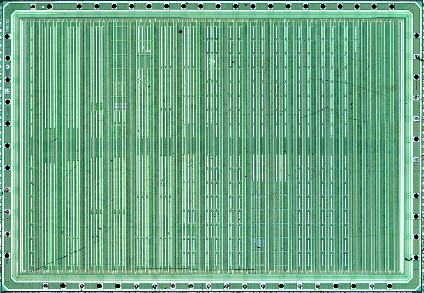
Decapped TT06 die - individual projects are obscured by the vertical power rails
That makes it hard to see your artwork (or anyone else’s logic) with the naked eye or a basic microscope. Tiny Tapeout has a partnership with Texplained: they remove the top metal layer and capture high-resolution microscope images of the die underneath. Here is the same TT06 chip after delayering — the individual project blocks and routing are clearly visible:
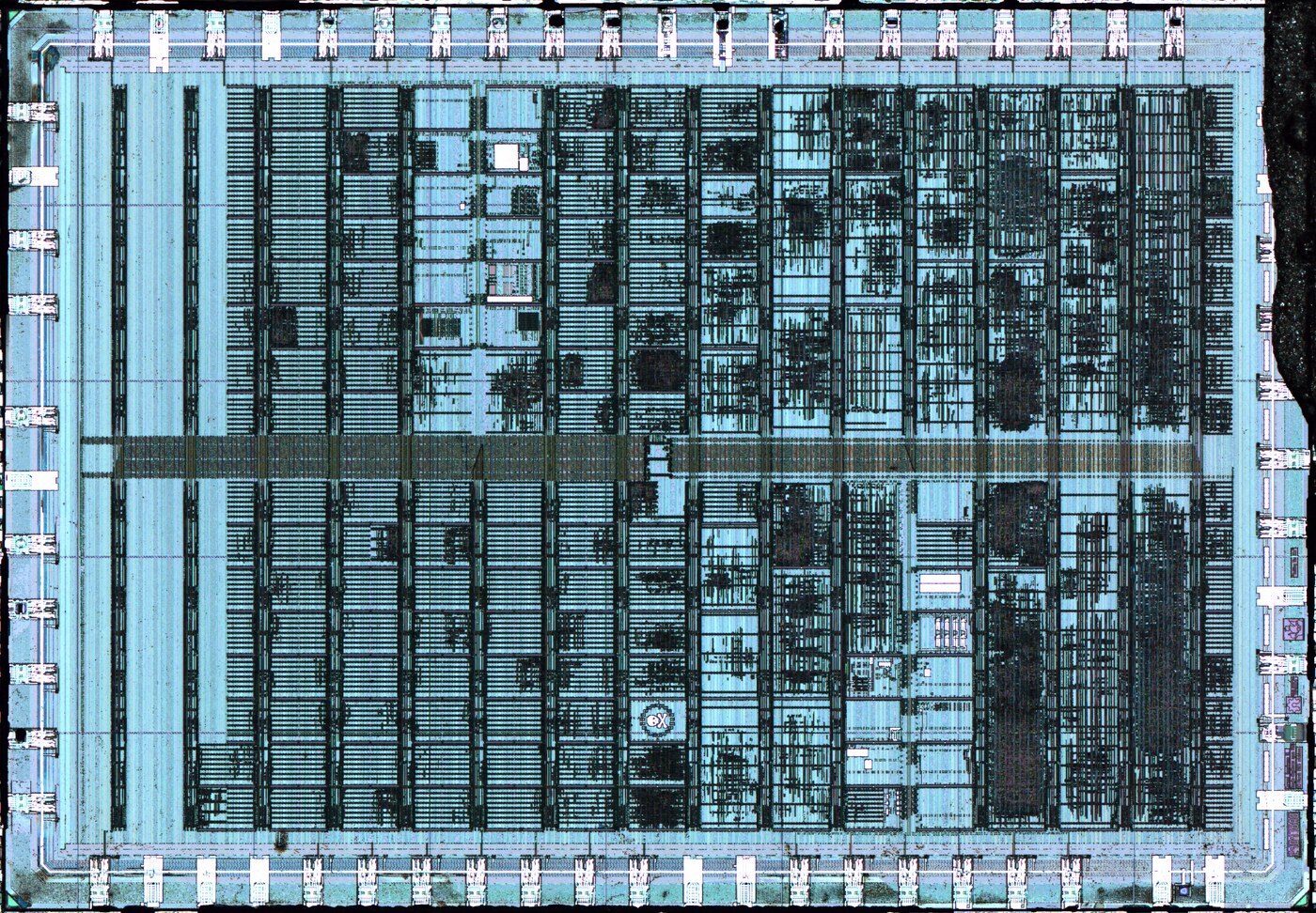
TT06 with the top metal layer removed
If you look closely, you will find a skull silicon art hidden among the tiles. Here is a close-up of that design after delayering:
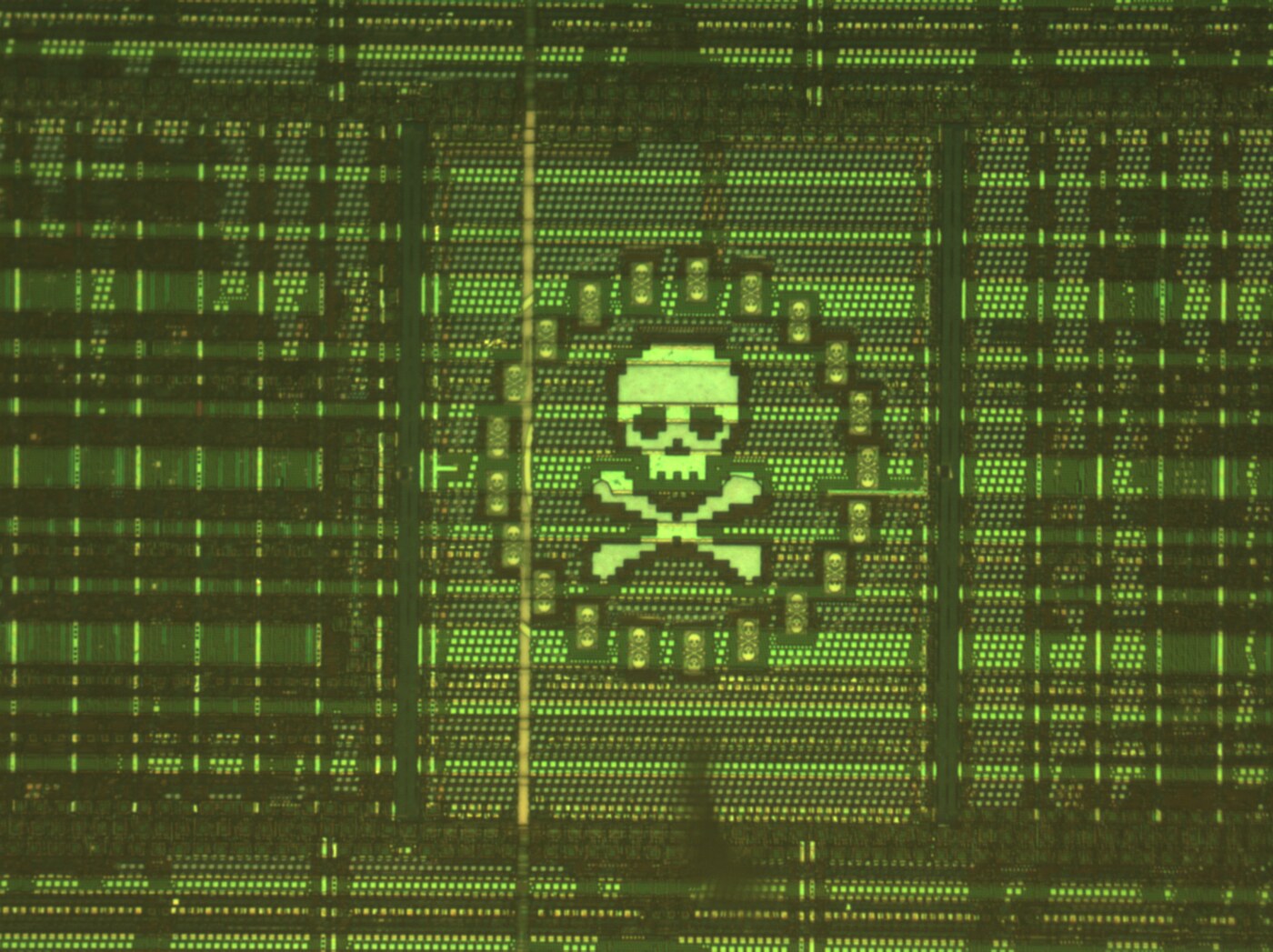
Uri Shaked's "Oscillating Bones" project built with "SkullFET" transistors
You can explore the full TT06 imaging data in the interactive chip viewer — zoom and pan across the entire shuttle to find your tile and any silicon art on it.
Creating art from code
If you don’t have art prepared in a layout editor, you can generate GDS files with Python. The gdstk library is a good choice.
Two complete working generators are available as reference:
- IHP shuttles — weaving01/macro_generation/generation.py: woven structure on TopMetal1 with fill layers
- SKY shuttles — crossstitching01/macro_generation/generation.py: cross-stitch tiles on met4
The walkthrough below distils the important parts of each.
Install gdstk
pip install gdstk
Minimal example (IHP)
This script follows the same structure as the weaving01 generator: art on TopMetal1, a PR boundary, then GDS + LEF output.
import gdstk

CELL_NAME = "my_logo"

# IHP SG13G2 layers (see table below)
ART_LAYER = 126              # TopMetal1
BOUNDARY_LAYER, BOUNDARY_DATATYPE = 189, 4  # prBoundary

def write_lef(filename, cell_name, bounds):
    """Write a minimal LEF file. bounds = (xmin, ymin, xmax, ymax)."""
    width = bounds[2] - bounds[0]
    height = bounds[3] - bounds[1]
    with open(filename, "w") as f:
        f.write(f"# LEF file generated for {cell_name}\n")
        f.write("VERSION 5.8 ;\n")
        f.write("NAMESCASESENSITIVE ON ;\n")
        f.write("DIVIDERCHAR \"/\" ;\n")
        f.write("BUSBITCHARS \"[]\" ;\n")
        f.write("UNITS\n")
        f.write("   DATABASE MICRONS 1000 ;\n")
        f.write("END UNITS\n\n")
        f.write(f"MACRO {cell_name}\n")
        f.write("   CLASS BLOCK ;\n")
        f.write(f"   FOREIGN {cell_name} 0 0 ;\n")
        f.write(f"   SIZE {width:.3f} BY {height:.3f} ;\n")
        f.write("   SYMMETRY X Y ;\n")
        f.write(f"END {cell_name}\n")


lib = gdstk.Library()
cell = lib.new_cell(CELL_NAME)

cell_width, cell_height = 120, 80

# PR boundary — required for macro placement
cell.add(gdstk.rectangle(
    (0, 0), (cell_width, cell_height),
    layer=BOUNDARY_LAYER, datatype=BOUNDARY_DATATYPE,
))

# Simple art: one TopMetal1 rectangle
cell.add(gdstk.rectangle((10, 10), (50, 30), layer=ART_LAYER))

cell.write_svg("../macros/my_logo.svg")
lib.write_gds("../macros/my_logo.gds")

bounds = (0, 0, cell_width, cell_height)
write_lef("../macros/my_logo.lef", CELL_NAME, bounds)
Run the script from a macro_generation/ folder (or adjust the output paths), then continue from Step 2.
Minimal example (SKY)
This script follows the same structure as the crossstitching01 generator: art on met4, a PR boundary, then GDS + LEF output.
import gdstk

CELL_NAME = "my_logo"

# SKY130 layers (see table below)
ART_LAYER, ART_DATATYPE = 71, 20   # met4.drawing
BOUNDARY_LAYER, BOUNDARY_DATATYPE = 235, 4  # prBoundary


def write_lef(filename, cell_name, bounds):
    """Write a minimal LEF file. bounds = (xmin, ymin, xmax, ymax)."""
    width = bounds[2] - bounds[0]
    height = bounds[3] - bounds[1]
    with open(filename, "w") as f:
        f.write(f"# LEF file generated for {cell_name}\n")
        f.write("VERSION 5.8 ;\n")
        f.write("NAMESCASESENSITIVE ON ;\n")
        f.write("DIVIDERCHAR \"/\" ;\n")
        f.write("BUSBITCHARS \"[]\" ;\n")
        f.write("UNITS\n")
        f.write("   DATABASE MICRONS 1000 ;\n")
        f.write("END UNITS\n\n")
        f.write(f"MACRO {cell_name}\n")
        f.write("   CLASS BLOCK ;\n")
        f.write(f"   FOREIGN {cell_name} 0 0 ;\n")
        f.write(f"   SIZE {width:.3f} BY {height:.3f} ;\n")
        f.write("   SYMMETRY X Y ;\n")
        f.write(f"END {cell_name}\n")


lib = gdstk.Library()
cell = lib.new_cell(CELL_NAME)

cell_width, cell_height = 80, 60

# PR boundary — required for macro placement
cell.add(gdstk.rectangle(
    (0, 0), (cell_width, cell_height),
    layer=BOUNDARY_LAYER, datatype=BOUNDARY_DATATYPE,
))

# Simple art: one met4 rectangle
cell.add(gdstk.rectangle(
    (10, 10), (50, 30),
    layer=ART_LAYER, datatype=ART_DATATYPE,
))

cell.write_svg("../macros/my_logo.svg")
lib.write_gds("../macros/my_logo.gds")

bounds = (0, 0, cell_width, cell_height)
write_lef("../macros/my_logo.lef", CELL_NAME, bounds)
Run the script from a macro_generation/ folder (or adjust the output paths), then continue from Step 2.
Open the SVG preview to check your art before running the full GDS build. It’s much faster to iterate on shapes in Python than to wait for the GitHub Action each time.
Avoid ellipse, text, and other helpers that produce curved or arbitrary geometry — they may look fine in the SVG preview but fail DRC.
Fill pattern for IHP shuttles
Large IHP macros may fail density checks without fill shapes underneath the art. One example for a fill pattern can be found in the weaving01 generator. It adds a grid of active and poly rectangles for this purpose — see the layer numbers in the table below. Small art macros like the minimal example above may not need fill at all.
Layer and datatype numbers
Each shuttle uses specific GDS layer and datatype numbers. Using the wrong values means your art won’t appear on the expected metal layer, or the precheck may reject the file.
The values below match the working generators for each PDK:
IHP shuttles
| Purpose | Layer | Datatype | Notes |
|---|---|---|---|
| Art (TopMetal1) | 126 | 0 | Minimum width/spacing ~1.64 µm |
| PR boundary | 189 | 4 | Place-and-route footprint; required in the macro GDS |
| Active filler | 1 | 22 | For density on larger macros |
| Poly rect filler | 5 | 22 | Paired with active filler |
SKY shuttles
| Purpose | Layer | Datatype | Notes |
|---|---|---|---|
| Art (met4) | 71 | 20 | Highest metal in the standard TT digital flow |
| PR boundary | 235 | 4 | Place-and-route footprint; required in the macro GDS |
Troubleshooting
| Problem | Things to check |
|---|---|
| GDS action fails with “macro not found” | Cell name in GDS, LEF, config.json, and project.v must all match exactly |
| Art doesn’t appear in preview | Wrong layer/datatype for your shuttle; open the GDS in a viewer like KLayout to confirm shapes exist |
| Disconnected pin / module errors | Add macro and instance names to IGNORE_DISCONNECTED_MODULES; set "ERROR_ON_DISCONNECTED_PINS": false |
| Art overlaps power stripes | Adjust FP_PDN_VOFFSET and/or move the macro location |
| IHP DRC / density failures on large art | Add the fill pattern under your macro |
| SKY DRC failures on met4 art | Check minimum width/spacing rules for met4 |
If you’re stuck, ask in the Tiny Tapeout Discord — many participants have added silicon art before and can help debug placement issues.