974 LISA 8-Bit Microcontroller
974 : LISA 8-Bit Microcontroller
- Author: Ken Pettit
- Description: 8-Bit Microcontroller SOC with 128 bytes DFFRAM module
- GitHub repository
- Open in 3D viewer
- Clock: 22000000 Hz
- Feedback: ✅ 1
LISA Overview?
LISA is a Microcontroller built around a custom 8-Bit Little ISA (LISA) microprocessor core. It includes several standard peripherals that would be found on commercial microcontrollers including timers, GPIO, UARTs and I2C. The following is a block diagram of the LISA Microcontroller:
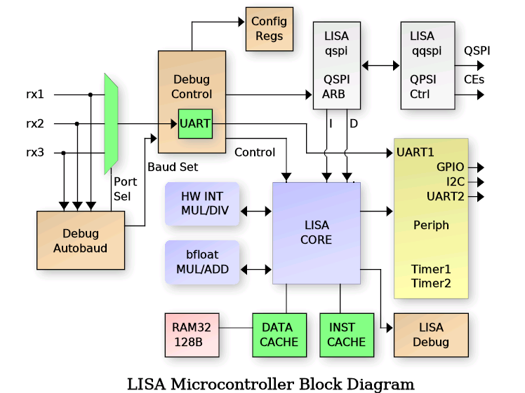
- The LISA Core has a minimal set of register that allow it to run C programs:
- Program Counter + Return Address Resister
- Stack Pointer and Index Register (Indexed DATA RAM access)
- 8-bit Accumulator + 16-bit BF16 Accumulator and 4 BF16 registers
Deailed list of the features
- Harvard architecture LISA Core (16-bit instruction, 15-bit address space)
- Debug interface
- UART controlled
- Auto detects port from one of 3 interfaces
- Auto detects the baud rate
- Interfaces with SPI / QSPI SRAM or FLASH
- Can erase / program the (Q)SPI FLASH
- Read/write LISA core registers and peripherals
- Set LISA breakpoints, halt, resume, single step, etc.
- SPI/QSPI programmability (single/quad, port location, CE selects)
- (Q)SPI Arbiter with 3 access channels
- Debug interface for direct memory access
- Instruction fetch
- Data fetch
- Quad or Single SPI. Hereafter called QSPI, but supports either.
- Onboard 128 Byte RAM for DATA / DATA CACHE
- Data bus CACHE controller with 8 16-byte CACHE lines
- Instruction CACHE with a single 4-instruction CACHE line
- Two 16-bit programmable timers (with pre-divide)
- Debug UART available to LISA core also
- Dedicated UART2 that is not shared with the debug interface
- 8-bit Input port (PORTA)
- 8-bit Output port (PORTB)
- 4-bit BIDIR port (PORTC)
- I2C Master controller
- Hardware 8x8 integer multiplier
- Hardware 16/8 or 16/16 integer divider
- Hardware Brain Float 16 (BF16) Multiply/Add/Negate/Int16-to-BF16
- Programmable I/O mux for maximum flexibility of I/O usage.
It uses a 32x32 1RW DFFRAM macro to implement a 128 bytes (1 kilobit) RAM module. The 128 Byte ram can be used either as a DATA cache for the processor data bus, giving a 32K Byte address range, or the CACHE controller can be disabled, connecting the Lisa processor core to the RAM directly, limiting the data space to 128 bytes. Inclusion of the DFFRAM is thanks to Uri Shaked (Discord urish) and his DFFRAM example.
Reseting the project does not reset the RAM contents.
Connectivity
All communication with the microcontroller is done through a UART connected to the Debug Controller. The UART I/O pins are auto-detected by the debug_autobaud module from the following choices (RX/TX):
ui_in[3]  / ui_out[4]     RP2040 UART interface
uio_in[4] / uio_out[5]    LISA PMOD board (I am developing)
uio_in[6] / uio_out[5]    Standard UART PMOD
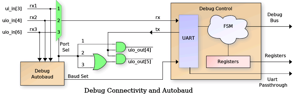
The RX/TX pair port is auto-detected after reset by the autobaud circuit, and the UART baud rate can either be configured manually or auto detected by the autobaud module. After reset, the ui_in[7] pin is sampled to determine the baud rate selection mode. If this input pin is HIGH, then autobaud is disabled and ui_in[6:0] is sampled as the UART baud divider and written to the Baud Rate Generator (BRG). The value of this divider should be: clk_freq / baud_rate / 8 - 1. Due to last minute additions of complex floating point operations, and only 2 hours left on the count-down clock, the timing was relaxed to 20MHz input clock max. So for a 20MHz clock and 115200 baud, the b_div[6:0] value would be 42 (for instance).
If the ui_in[7] pin is sampled LOW, then the autobaud module will monitor all three potential RX input pins for LINEFEED (ASCII 0x0A) code to detect baud rate and set the b_div value automatially. It monitors bit transistions and searches for three successive bits with the same bit period. Since ASCII code 0x0A contains a "0 1 0 1 0" bit sequence, the baud rate can be detected easily.
Regardless if the baud rate is set manually or using autobaud, the input port selection will be detect automatically by the autobaud. In the case of manual buad rate selection, it simply looks for the first transition on any of the three RX pins. For autobaud, it select the RX line with three successive eqivalent bit periods.
Debug Interface Details
The Debug interface uses a fixed, verilog coded Finite State Machine (FSM) that supports a set of commands over the UART to interface with the microcontroller. These commands are simple ASCII format such that low-level testing can be performed using any standard terminal software (such as minicom, tio. Putty, etc.). The 'r' and 'w' commands must be terminated using a NEWLINE (0x0A) with an optional CR (0x0D). Responses from the debug interface are always terminated with a LINFEED plus CR sequence (0x0A, 0x0D). The commands are as follows (responsce LF/CR ommited):
| Command | Description |
|---|---|
| v | Report Debugger version. Should return: lisav1.2 |
| wAAVVVV | Write 16-bit HEX value 'VVVV' to register at 8-bit HEX address 'AA'. |
| rAA | Read 16-bit register value from 8-bit HEX address 'AA'. |
| t | Reset the LISA core. |
| l | Grant LISA the UART. Further data will be ignored by the debugger. |
| +++ | Revoke LISA UART. NOTE: a 0.5s guard time before/after is required. |
NOTE: All HEX values must be a-f and not A-F. Uppercase is not supported.
Debug Configuration and Control Registers
The following table describes the configuration and LISA debug register addresses available via the debug 'r' and 'w' commands. The individual register details will be described in the sections to follow.
| ADDR | Description | ADDR | Description |
|---|---|---|---|
| 0x00 | LISA Core Run Control | 0x12 | LISA1 QSPI base address |
| 0x01 | LISA Accumulator / FLAGS | 0x13 | LISA2 QSPI base address |
| 0x02 | LISA Program Counter (PC) | 0x14 | LISA1 QSPI CE select |
| 0x03 | LISA Stack Pointer (SP) | 0x15 | LISA2 QSPI CE select |
| 0x04 | LISA Return Address (RA) | 0x16 | Debug QSPI CE select |
| 0x05 | LISA Index Register (IX) | 0x17 | QSPI Mode (QUAD, flash, 16b) |
| 0x06 | LISA Data bus | 0x18 | QSPI Dummy read cycles |
| 0x07 | LISA Data bus address | 0x19 | QSPI Write CMD value |
| 0x08 | LISA Breakpoint 1 | 0x1a | The '+++' guard time count |
| 0x09 | LISA Breakpoint 2 | 0x1b | Mux bits for uo_out |
| 0x0a | LISA Breakpoint 3 | 0x1c | Mux bits for uio |
| 0x0b | LISA Breakpoint 4 | 0x1d | CACHE control |
| 0x0c | LISA Breakpoint 5 | 0x1e | QSPI edge / SCLK speed |
| 0x0d | LISA Breakpoint 6 | 0x20 | Debug QSPI Read / Write |
| 0x0f | LISA Current Opcode Value | 0x21 | Debug QSPI custom command |
| 0x10 | Debug QSPI Address (LSB16) | 0x22 | Debug read SPI status reg |
| 0x11 | Debug QSPI Address (MSB8) |
LISA Processor Interface Details
The LISA Core requires external memory for all Instructions and Data (well, sort of for data, the data CACHE can be disabled then it just uses internal DFFRAM). To accomodate external memory, the design uses a QSPI controller that is configurable as either single SPI or QUAD SPI, Flash or SRAM access, 16-Bit or 24-Bit addressing, and selectable Chip Enable for each type of access. To achieve this, a QSPI arbiter is used to allow multiple accessors as shown in the following diagram:
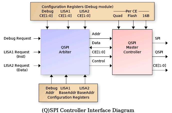
The arbiter is controlled via configuration registers (accessible by the Debug controller) that specify the operating mode per CE, and CE selection bits for each of the three interfaces:
- Debug Interface
- LISA1 (Instruction fetch)
- LISA2 (Data read/write)
The arbiter gives priority to the Debug accesses and processes LISA1 and LISA2 requests using a round-robbin approach. Each requestor provides a 24-bit address along with 16-bit data read/write. For the Debug interface, the address comes from the configuration registers directly. For LISA1, the address is the Program Counter (PC) + LISA1 Base and for LISA2, it is the Data Bus address + LISA2 Base. The LISA1 and LISA2 base addresses are programmed by the Debug controller and set the upper 16-bits in the 24-bit address range. The PC and Data address provide the lower 16 bis (8-bits overlapped that are 'OR'ed together). The BASE addresses allow use of a single external QSPI SRAM for both instruction and data without needing to worry about data collisions.
When the arbiter chooses a requestor, it passes its programmed CE selection to the QSPI controller. The QSPI controller then uses the programmed QUAD, MODE, FLASH and 16B settings for the chosen CE to process the request. This allows LISA1 (Instruction) to either execute from the same SRAM as LISA2 (Data) or to execute from a separate CE (such as FLASH with permanent data storage).
Additionally the Debug interface has special access registers in the 0x20 - 0x22 range that allow special QSPI accesses such as FLASH erase and program, SRAM programming, FLASH status read, etc. In fact the Debug controller can send any arbitrary command to a target device, using access that either provide an associated address (such as erase sector) or no address. The proceedure for this is:
- Program Debug register 0x19 with the special 8-bit command to be sent
- Set the 9-th bit (reg19[8]) to 1 if a 16/24 bit address needs to be sent)
- Perform a read / write operation to debug address 0x21 to perform the action.
Simple QSPI data reads/write are accomplished via the Debug interface by setting the desired address in Debug config register 0x10 and 0x11, then performing read or write to address 0x20 to perform the request. Reading from Debug config register 0x22 will perform a special mode read of QSPI register 0x05 (the FLASH status register).
Data access to the QSPI arbiter come from the Data CACHE interface (described later), enabling a 32K address space for data. However the design has a CACHE disable mode that directs all Data accesses directly to the internal 128 Byte RAM, thus eliminating the need for external SRAM (and limiting the data bus to 128 bytes).
Programming the QSPI Controller
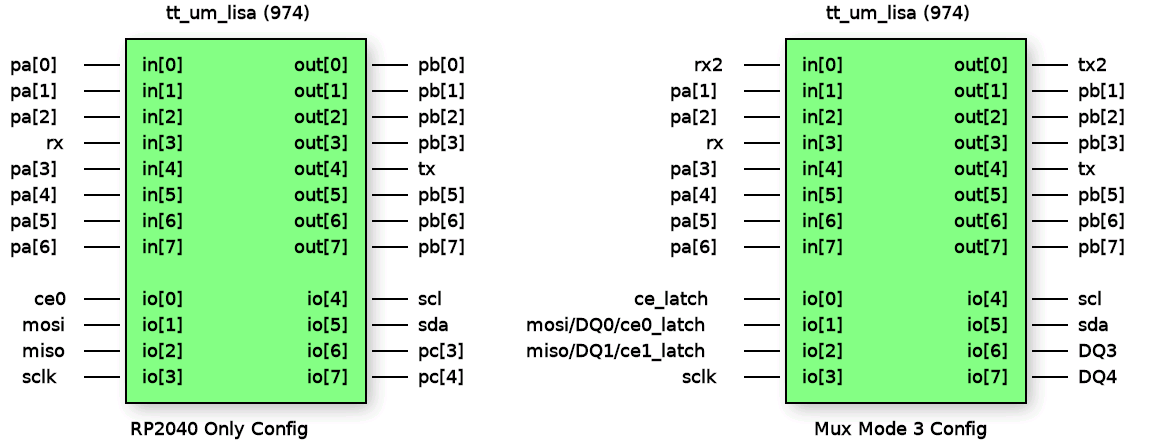
Before the LISA microcontroller can be used in any meaningful manner, a SPI / QSPI SRAM (and optionally a NOR FLASH) must be connected to the Tiny Tapeout PCB. Alternately, the RP2040 controller on the board can be configured to emulate a single SPI (the details for configuring this are outside the scope of this documentation ... search the Tiny Tapeout website for details.). For the CE signals, there are two operating modes, fixed CE output and Mux Mode 3 "latched" CE mode. Both will be described here. The other standard SPI signals are routed to dedicated pins as follows:
| Pin | SPI | QSPI | Notes |
|---|---|---|---|
| uio[0] | CE0 | CE0 | |
| uio[1] | MOSI | DQ0 | Also MOSI prior to QUAD mode DQ0 |
| uio[2] | MISO | DQ1 | Also MISO prior to QUAD mode DQ1 |
| uio[3] | SCLK | SCLK | |
| uio[4] | CE1 | CE1 | Must be enabled via uio MUX bits |
| uio[6] | - | DQ2 | Must be enabled via uio MUX bits |
| uio[7] | - | DQ3 | Must be enabled via uio MUX bits |
For Special Mux Mode 3 (Debug register 0x1C uio_mux[7:6] = 2'h3), the pinout is mostly the same except the CE signals are not constant. Instead they are "latched" into an external 7475 type latch. This mode is to support a PMOD board connected to the uio PMOD which supports a QSPI Flash chip, a QSPI SRAM chip, and either Debug UART or I2C. For all of that functionality, nine pins would be required for continuous CE0/CE1, however only eight are available. So the external PMOD uses uio[0] as a CE "latch" signal and the CE0/CE1 signals are provided on uio[1]/uio[2] during the latch event. This requires a series resistor as indicated to allow CE updates if the FLASH/SRAM is driving DQ0/DQ1. The pinout then becomes:
| Pin | SPI/QSPI | Notes |
|---|---|---|
| uio[0] | ce_latch | ce_latch HIGH at beginning of cycle |
| uio[1] | ce0_latch/MOSI/DQ0 | Connection to FLASH/SRAM via series resistor |
| uio[2] | ce1_latch/MISO/DQ1 | Connection to FLASH/SRAM via series resistor |
| uio[3] | SCLK | |
| uio[6] | -/DQ2 | Must be enabled via uio MUX bits |
| uio[7] | -/DQ3 | Must be enabled via uio MUX bits |
This leaves uio[4]/uio[5] available for use as either UART or I2C.
Once the SPI/QSPI SRAM and optional FLASH have been chosen and connected, the Debug configuration registers must be programmed to indicate the nature of the external device(s). This is accompilished using Debug registers 0x12 - 0x19 and 0x1C. To programming the proper mode, follow these steps:
-
Program the LISA1, LISA2 and Debug CE Select registers (0x14, 0x15, 0x16) indicating which CE to use.
- 0x14, 0x15, 0x16: {6'h0, ce1_en, ce0_en} Active HIGH
-
Program the LISA1 and LISA2 base addresses if they use the same SRAM:
- 0x12: {LISA1_BASE, 8'h0} | {8'h0, PC}
- 0x13: {LISA2_BASE, 8'h0} | {8'h0, DATA_ADDR}
-
Program the mode for each Chip Enable (bits active HIGH)
- 0x17: {10'h0, is_16b[1:0], is_flash[1:0], is_quad[1:0]}
-
For Quad SPI, Special Mux Mode 3, or CE1, program the uio_mux mode:
- 0x1C:
- [7:6] = 2'h2: Normal QSPI DQ2 select
- [7:6] = 2'h3: Special Mux Mode 3 (Latched CE)
- [5:4] = 2'h2: Normal QSPI DQ3 select
- [5:4] = 2'h3: Special Mux Mode 3
- [1:0] = 2'h2: CE1 select on uio[4]
- 0x1C:
-
For RP2040, you might need to slow down the SPI clock / delay between successive CE activations:
- 0x1E:
- [3:0] spi_clk_div: Number of clocks SCLK HIGH and LOW
- [10:4] ce_delay: Number clocks between CE activations
- [12:11] spi_mode: Per-CE FALLING SCLK edge data update
- 0x1E:
-
Set the number of DUMMY ready required for each CE:
- 0x18: {8'h0, dummy1[3:0], dummy0[3:0]
-
For QSPI FLASH, set the QSPI Write opcode (it is different for various Flashes):
- 0x19: {8'h0, quad_write_cmd}
NOTE: For register 0x1E (SPI Clock Div and CE Delay), there is only a single register, meaning this register value applies to both CE outputs. Delaying the clock of one CE will delay both, and adding delay between CE activations does not keep track of which CE was activated. So if two CE outputs are used and a CE delay is programmed, it will enforce that delay even if a different CE is used. This setting is really in place for use when the RP2040 emulation is being used in a single CE SRAM mode only (i.e. you have no external PMOD with a real SRAM / FLASH chip. In the case of real chips on a PMOD, SCLK and CE delays (most likely) are not needed. The Tech Page on the Tiny Tapeout regarding RP2040 SPI SRAM emulation indicates a delay between CE activations is likely needed, so this setting is provided in case it is needed.
Architecture Details
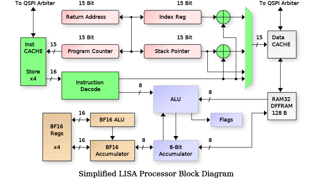
Below is a simplified block diagram of the LISA processor core. It uses an 8-bit accumulator for most of its operations with the 2nd argument predominately coming from either immediate data in the instruction word or from a memory location addressed by either the Stack Pointer (SP) or Index Register (IX).
There are also instructions that work on the 15-bit registers PC, SP, IX and RA (Return Address). As well as floating point operations. These will be covered in the sections to follow.
Addressing Modes
Like most processors, LISA has a few different addressing modes to get data in and out of the core. These include the following:
| Mode | Data | Description |
|---|---|---|
| Register | Rx[n -: 8] | Transfers between registers (ix, ra, facc, etc.). |
| Direct | inst[n:0] | N-bit data stored in the instruction word. |
| NextOp | (inst+1)[14:0] | Data stored in the NEXT instruction word. |
| Indirect | mem[inst[n:0]] | Address of the data is in the instruction word. |
| Periph | periph[inst[n:0]] | Accesses to the peripheral bus. |
| Indexed | mem[sp/ix+inst[n:0]] | The SP or IX register is added to a fixed offset. |
| Stack | mem[sp] | Stack pointer points to the data (push/pop). |
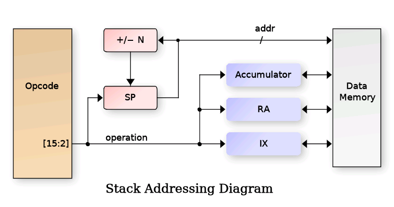
The Control Registers
To run meaninful programs, the Program Counter (PC) and Stack Pointer (SP) must be set to useful values for accessing program instructions and data. The PC is automatically reset to zero by rst_n, so that one is pretty much automatic. All programs start at address zero (plus any base address programmed by the Debug Controller). But as far as the LISA core is concerned, it knows nothing of base addresses and believes it is starting at address zero.
Next is to program the SP to point to a useful location in memory. The Stack is a place where C programs store their local variable values and also where we store the Return Address (RA) if we need to call nested routines, etc. The stack grows down, meaning it starts at a high RAM address and decrements as things are added to the stack. Therefore the SP should be programmed with an address in upper RAM. LISA supports different Data bus modes through it's CACHE controller, including CACHE disable where it can only access 128 bytes. But for this example, let's assume we have a full range of 32K SRAM available. The LISA ISA doesn't have an opcode for loading the SP directly. Instead it can load the IX register directly with a 15-bit value using NextOp addressing, and it supports "xchg" opcodes to exchange the IX register with either the SP or RA. So to load the SP, we would write:
Example:
  ldx     0x7FFF      // Load IX with value in next opcode
  xchg_sp             // Exchange IX with SP
The IX register can be programmed as needed to access other data within the Data Bus address range. This register is useful especially for accessing structures via a C pointer. The IX then becomes the value of the pointer to RAM, and Indexed addressing mode allows fixed offsets from that pointer (i.e. structure elements) to be accessed for read/write.
Loading the PC indirectly can be done using the "jmp ix" opcode which does the operation pc <= ix. Loading ix from the pc directly is not supported, though this can be accomplished using a function call and opcodes to save RA (sra) and pop ix:
 Example:
   get_pc:
     sra         // Push RA to the stack (Save RA)
     pop_ix      // Pop IX from the stack
     ret         // Return. Upon return, IX is the same as PC
Conditional Flow Processing
Program flow is controlled using flags (zero, carry, sign), arithemetic mode (amode) and condition flags (cond) to determine when program branches should occur. Specific opcode update the flags and condition registers based on results of the operation (AND, OR, IF, etc.). Then conditional branches are made using bz, bnz and if (and variants ifte "if-then-else" and iftt "if-then-then"). Also available are rc "Return if Carry" and rz "Return if Zero", though these are less useful in C programs as typically a routine uses local variables and the stack must be restored prior to return, mandating a branch to the function epilog to restore the stack and often the return address. Below is a list of the opcodes used for conditional program processing:
Legend for operations below:
- acc_val = inst[7:0]
- pc_jmp = inst[14:0]
- pc_rel = pc + sign_extend(inst[10:0])
| Opcode | Operation | Encoding | Description |
|---|---|---|---|
| jal | pc <= pc_jmp | 0aaa_aaaa_aaaa_aaaa | Jump And Link (call). |
| ra <= pc | |||
| ret | pc <= ra | 1000_1010_0xxx_xxxx | Return |
| reti | pc <= ra | 1000_11xx_iiii_iiii | Return Immediate. |
| acc <= acc_val | |||
| br | pc <= pc_rel | 1011_0rrr_rrrr_rrrr | Branch Always |
| bz | pc <= pc_rel | 1011_1rrr_rrrr_rrrr | Branch if Zero. |
| if zero=1 | |||
| bnz | pc <= pc_rel | 1010_1rrr_rrrr_rrrr | Branch if Not Zero. |
| if zero=0 | |||
| rc | pc <= ra | 1000_1011_0xxx_xxxx | Return if Carry |
| if carry=1 | |||
| rz | pc <= ra | 1000_1011_1xxx_xxxx | Return if Zero |
| if zero=1 | |||
| call_ix | pc <= ix | 1000_1010_100x_xxxx | Call indirect via IX |
| ra <= pc | |||
| jump_ix | pc <= ix | 1000_1010_101x_xxxx | Jump indirect via IX |
| if | cond <= ?? | 1010_0010_0000_0ccc | If. See below. |
| iftt | cond <= ?? | 1010_0010_0000_1ccc | If then-then. See below. |
| ifte | cond <= ?? | 1010_0010_0001_0ccc | If then-else. See below. |
The IF Opcode
The "if" opcode and it's variants "if-then-then" and "if-then-else" control program flow in a slightly different manner than the others. Instead of affecting the value of the PC directly, they set the two condition bits "cond[1:0]" to indicate which (if any) of the two following opcodes should be executed. the cond[0] bit represents the next instruction and cond[1] represents the instruction following that. All three "if" forms take an argument that checks the current value of the FLAGS to set the condition bits. The argument is encoded as the lower three bits of the instruction word ard operate as shown in the following table:
| Condition | Test | Encoding | Description |
|---|---|---|---|
| EQ | zflag=1 | 3'h0 | Execute if Equal |
| NE | zflag=0 | 3'h1 | Execute if Not Equal |
| NC | cflag=0 | 3'h2 | Execute if Not Carry |
| C | cflag=1 | 3'h3 | Execute if Carry |
| GT | ~cSigned & ~zflag | 3'h4 | Execute if Greater Than |
| LT | cSigned & ~zflag | 3'h5 | Execute if Less Than |
| GTE | ~cSigned | zflag | 3'h6 |
| LTE | cSigned | zflag | 3'h7 |
The "if" opcode will set cond[0] based on the condition above and the cond[1] bit to HIGH. It only affects the single instruction following the "if" opcode. The "iftt" opcode will set both cond[0] and cond[1] to the same value based on the condition above. It means "if true, execute the next two opcodes". And the "ifte" opcode will set cond[0] based on the condition above and cond[1] to the OPPOSITE value, meaning it will execute either the following instruction OR the one after that (then-else).
Example:
  ldi      0x41        // Load A immediate with ASCII 'A'
  cpi      0x42        // Compare A immediate with ASCII 'B'
  ifte     eq          // Test if the compare was "Equal"
  jal      L_equal     // Jump if equal
  jal      L_different // Jump if different
The above code will load the "jal L_equal" opcode but will not execute it since the compare was Not Equal. Then it will execute the "jal L_different" opcode. Note that if the compare were "ifte ne", it would call the L_equal function and then upon return would not execute the "L_different" opcode. This is because the cond[1] code is saved with the Return Address (RA) during the call and restored upon return. This means the FALSE cond[1] code would prevent the 2nd opcode from executing. As an opcode gets executed, the cond[1] value is shifted into the cond[0] location, and the cond[1] is loaded with 1'b1.
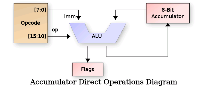
Direct Operations
To do any useful work, the LISA core must be able to load and operate on data. This is done through the accumulator using the various addressing modes. The diagram below details the Direct addressing mode where data is stored directly in the opcode / instruction word:
 \clearpage
The instructions that use direct addressing are:
\clearpage
The instructions that use direct addressing are:
| Opcode | Operation | Encoding | Description |
|---|---|---|---|
| adc | A <= A + imm + C | 1001_00xx_iiii_iiii | ADD immediate with Carry |
| ads | SP <= SP + imm | 1001_01ii_iiii_iiii | ADD SP + signed immediate |
| adx | IX <= IX + imm | 1001_10ii_iiii_iiii | ADD IX + signed immediate |
| andi | A <= A & imm | 1000_01xx_iiii_iiii | AND immediate with A |
| cpi | Z,C <= A >= imm | 1010_01xx_iiii_iiii | Compare A >= immediate |
| cpi | Z,C <= A >= imm | 1010_01xx_iiii_iiii | Compare A >= immediate |
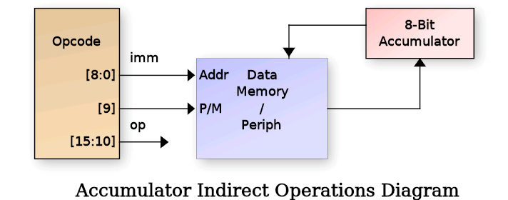
Accumulator Indirect Operations
The Accumulator Indirect operations use immediate data in the instruction word to index indirectly into Data memory. That memory address is then used to load, store or both load and store (swap) data with the accumulator.
| Opcode | Operation | Encoding | Description |
|---|---|---|---|
| lda | A <= M[imm] | 1111_01pi_iiii_iiii | Load A from Memory/Peripheral |
| sta | M[imm] <= A | 1111_11pi_iiii_iiii | Store A to Memory/Peripheral |
| swapi | A <= M[imm] | 1101_11pi_iiii_iiii | Swap Memory/Peripheral with A |
| M[imm] <= A |
- p = Select Peripheral (1'b1) or RAM (1'b0)
- iiii = Immediate data
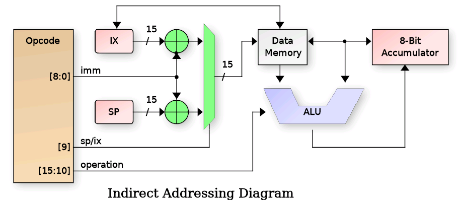
Indexed Operations
Indexed operations use either the IX or SP register plus a fixed offset from the immediate field of the opcode. The selection to use IX vs SP is also from the opcode[9] bit. The immediate field is not sign extended, so only positive direction indexing is supported. This was selected because this mode is typically used to access either local variables (when using SP) or C struct members (when using IX), and in both cases, negative index offsets aren't very useful. The following is a diagram of indexed addressing:
| Opcode | Operation | Encoding | Description |
|---|---|---|---|
| add | A <= A+ M[ind] | 1100_00si_iiii_iiii | ADD index memory to A |
| and | A <= A & M[ind] | 1101_00si_iiii_iiii | AND A with index memory |
| cmp | A >= M[ind]? | 1110_10si_iiii_iiii | Compare A with index memory |
| dcx | M[ind] -= 1 | 1001_11si_iiii_iiii | Decrement the value at index memory |
| inx | M[ind] += 1 | 1110_01si_iiii_iiii | Increment the value at index memory |
| ldax | A <= M[ind] | 1111_00si_iiii_iiii | Load A from index memory |
| ldxx | IX <= M[SP+imm] | 1100_110i_iiii_iiii | Load IX from memory at SP+imm |
| mul | A <= A*M[ind]L | 1100_10si_iiii_iiii | Multiply index memory * A, keep LSB |
| mulu | A <= A*M[ind]H | 1000_01si_iiii_iiii | Multiply index memory * A, keep MSB |
| or | A <= A | M[ind] | 1101_10si_iiii_iiii |
| stax | M[ind] <= A | 1111_10si_iiii_iiii | Store A to index memory |
| stxx | M[SP+imm] <= IX | 1100_111i_iiii_iiii | Save IX to memory at SP+imm |
| sub | A <= A-M[ind] | 1100_10si_iiii_iiii | SUBtract index memory from A |
| swap | A <= M[ind] | 1110_11si_iiii_iiii | Swap A with index memory |
| M[ind] <= A | |||
| xor | A <= A ^ M[ind] | 1110_00si_iiii_iiii | XOR A with index memory |
\clearpage Legend for table above:
- ind = IX or SP + immediate
- s = Select IX (zero) or SP (one)
- iiii = Immediate data
The Zero and Carry flags are updated for most of the above operations. The Carry flag is only updated for math operations where a Carry / Borrow could occur.
| Carry | Zero |
|---|---|
| adc | add and |
| add | or xor |
| sub | cmp sub |
| cmp | dcx inx |
| dcx | swap ldax |
| inx | mul mulu |
Stack Operations
Stack operations use the current value of the SP register to PUSH and POP items to the stack in opcode. As items are PUSHed to the stack, the SP is decremented after each byte, and as they are POPed, the SP is incremented prior to reading from RAM.
| Opcode | Operation | Encoding | Description |
|---|---|---|---|
| lra | RA <= M[SP+1] | 1010_0001_0110_01xx | Load {cond,RA} from stack |
| SP += 2 | |||
| sra | M[SP] <= RA | 1010_0001_0110_00xx | Save {cond,RA} to stack |
| SP -= 2 | |||
| push_ix | M[SP] <= IX | 1010_0001_0110_10xx | Save IX to stack |
| SP -= 2 | |||
| pop_ix | IX <= M[SP+1] | 1010_0001_0110_11xx | Load IX from stack |
| SP += 2 | |||
| push_a | M[SP] <= A | 1010_0000_100x_xxxx | Save A to stack |
| SP -= 1 | |||
| pop_a | A <= M[SP+1] | 1010_0000_110x_xxxx | Load A from stack |
| SP += 1 |
How to test
You will need to download and compile the C-based assembler, linker and C compiler I wrote (will make available) Also need to download the Python based debugger.
- Assembler is fully functional
- Includes limited libraries for crt0, signed int compare, math, etc.
- Libraries are still a work in progress
- Linker is fully functional
- C compiler is somewhat functional (no float support at the moment) but has many bugs in the generated code and is still a work in progress.
- Python debugger can erase/program the FLASH, program SPI SRAM, start/stop the LISA core, read SRAM and registers.
\clearpage
Legend for Pinout
- pa: LISA GPIO PortA Input
- pb: LISA GPIO PortB Output
- b_div: Debug UART baud divisor sampled at reset
- b_set: Debug UART baud divisor enable (HIGH) sampled at reset
- baud_clk: 16x Baud Rate clock used for Debug UART baud rate generator
- ce_latch: Latch enable for Special Mux Mode 3 as describe above
- ce0_latch: CE0 output during Special Mux Mode 3
- ce1_latch: CE1 output during Special Mux Mode 3
- DQ1/2/3/4: QUAD SPI bidirection data I/O
- pc_io: LISA GPIO Port C I/O (direction controllable by LISA)
IO
| # | Input | Output | Bidirectional |
|---|---|---|---|
| 0 | pa_in[0]/baud_div[0] | pb_out[0] | ce0/ce_latch |
| 1 | pa_in[1]/baud_div[1] | pb_out[1] | mosi/dq1/ce0 |
| 2 | pa_in[2]/baud_div[2] | pb_out[2] | miso/dq2/ce1 |
| 3 | pa_in[3]/baud_div[3]/rx | pb_out[3] | sclk |
| 4 | pa_in[4]/baud_div[4] | pb_out[4]/tx | rx /pc_io[0]/scl/sda |
| 5 | pa_in[5]/baud_div[5] | pb_out[5] | tx /pc_io[1]/sda/scl |
| 6 | pa_in[6]/baud_div[6] | pb_out[6] | scl /pc_io[2]/dq2/rx |
| 7 | pa_in[7]/baud_set | pb_out[7]/baud_clk | sda/pc_io[3]/dq3 |
User feedback
- kdp1965👑: Have Fully tested the LISA core, debugger, internal DFFRAM, SPI/QSPI to external FLASH and RP2040 emulated RAM, BrainFloat16 FPU, Timers, GPIO, Internal UART. Still left to test: I2C master and DFFRAM Cache controller.