5 74HCT00 Quad 2-Input NAND (3.3 V)
5 : 74HCT00 Quad 2-Input NAND (3.3 V)
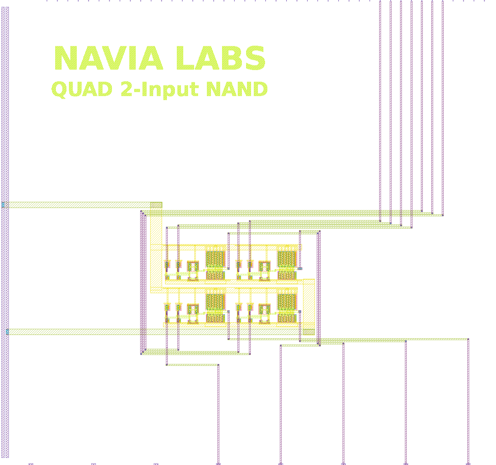
- Author: Vipul Sharma
- Description: Open-source silicon realization of 74HCT00 TTL-compatible quad 2-input NAND on gf180mcuD at 3.3 V
- GitHub repository
- Open in 3D viewer
- Open in Tiny Tapeout Explorer
- Clock: 0 Hz
How it works
This project is an open-source silicon implementation of quad 2-input NAND on the GlobalFoundries gf180mcuD process, operating from a 3.3 V supply. Each NAND gate presents a TTL-compatible input window (V<sub>IL,max</sub> = 0.8 V, V<sub>IH,min</sub> = 2.0 V) and is sized for ±4 mA drive at the output.
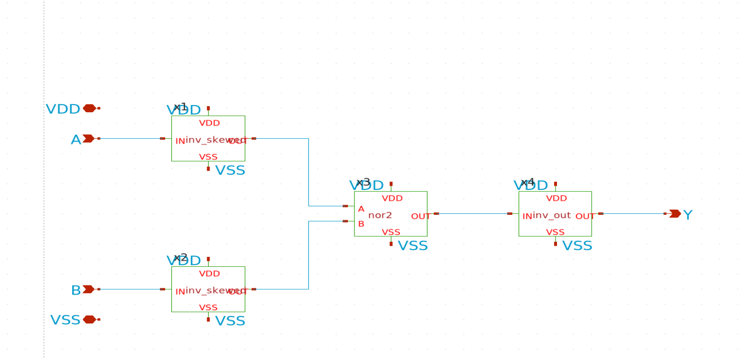
The HCT input behaviour is realised through a skewed-inverter / NOR2 / output-buffer chain rather than a plain CMOS NAND topology:
nand2\_hct  =  inv\_skewed (A) ─┐
              inv\_skewed (B) ─┴─►  nor2  ──►  inv\_out  ──►  Y
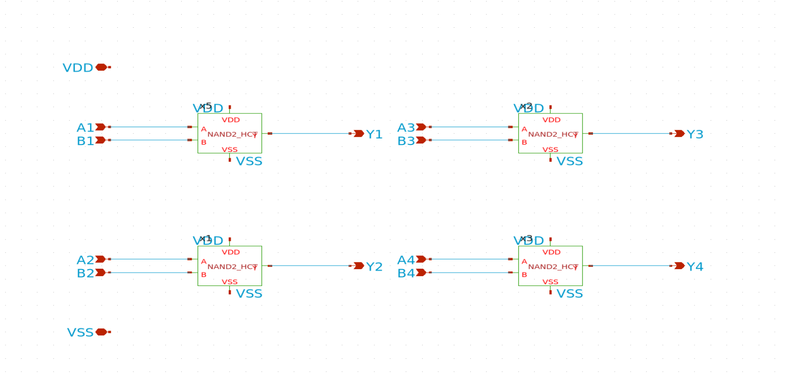
The four NAND gates share a common V<sub>DD</sub>/V<sub>SS</sub> rail pair.
Each gate output is routed to an analog pin in ua\[0..3] rather than to the
digital pins, allowing V<sub>OH</sub> and V<sub>OL</sub> to be measured at
the rated ±4 mA drive without the digital output buffer of the TT pad frame
in series.
Gate 1's A input (A<sub>1</sub>) is brought out exclusively on the
analog pin ua\[4] rather than on a digital ui\_in pin. This bypasses
the TT digital pad buffer entirely and is used for two purposes:
(a) functional drive at 0 V or 3.3 V for the truth-table test, and
(b) a slow DC ramp from 0 V to 3.3 V to characterise the HCT input
window on silicon. A digital ui\_in pin would otherwise snap any
intermediate voltage to a clean 0 V or 3.3 V at the TT pad buffer's
own CMOS threshold before it ever reached the gate, making the
HCT-window measurement impossible.
Schematics
The design was captured in xschem and simulated in ngspice. Per-cell LVS was performed in KLayout.
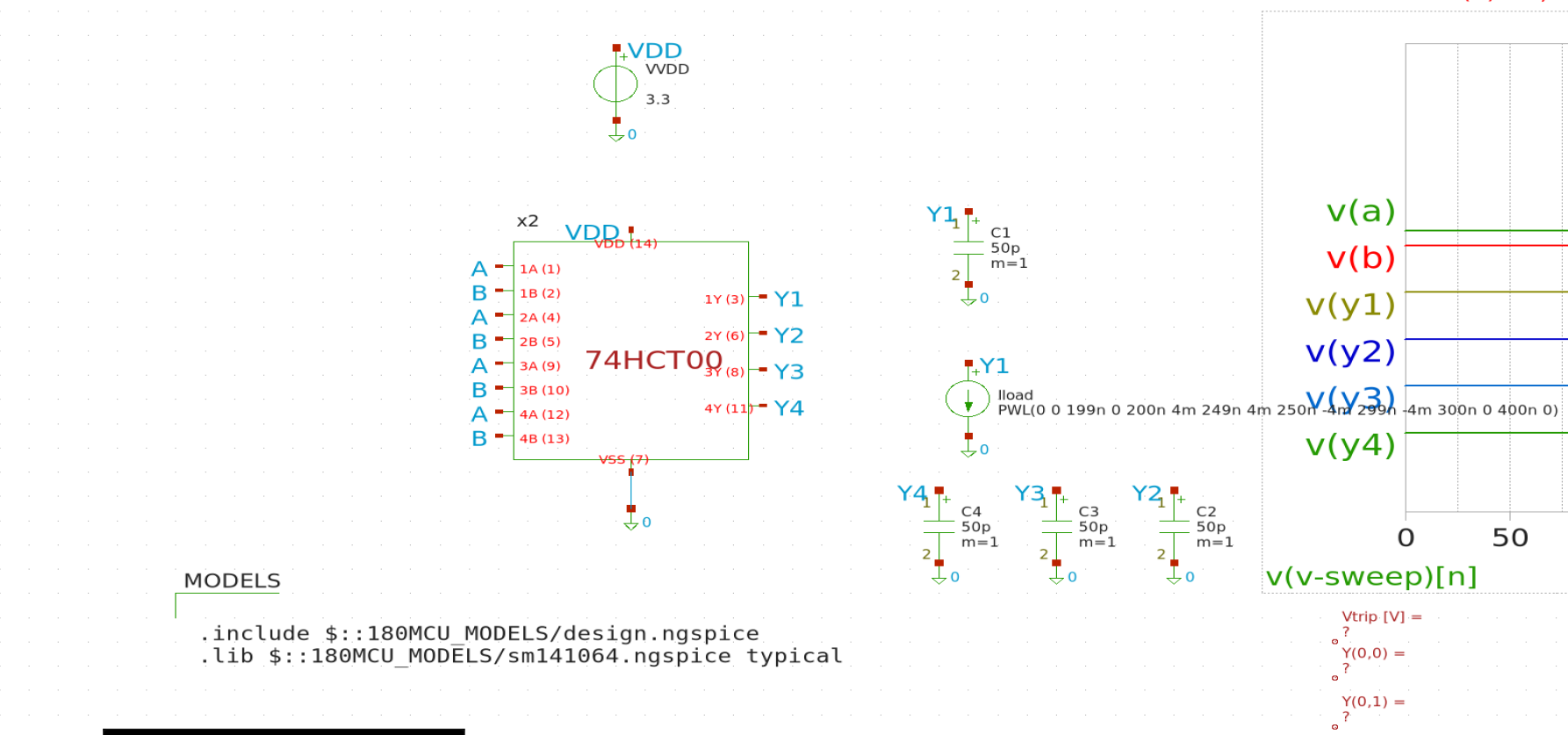
Chip-level testbench (tb\_74hct00\_top.sch):
Top-level schematic (74hct00\_top.sch):
NAND gate (nand2\_hct.sch):
Interior NOR2 (nor2.sch):
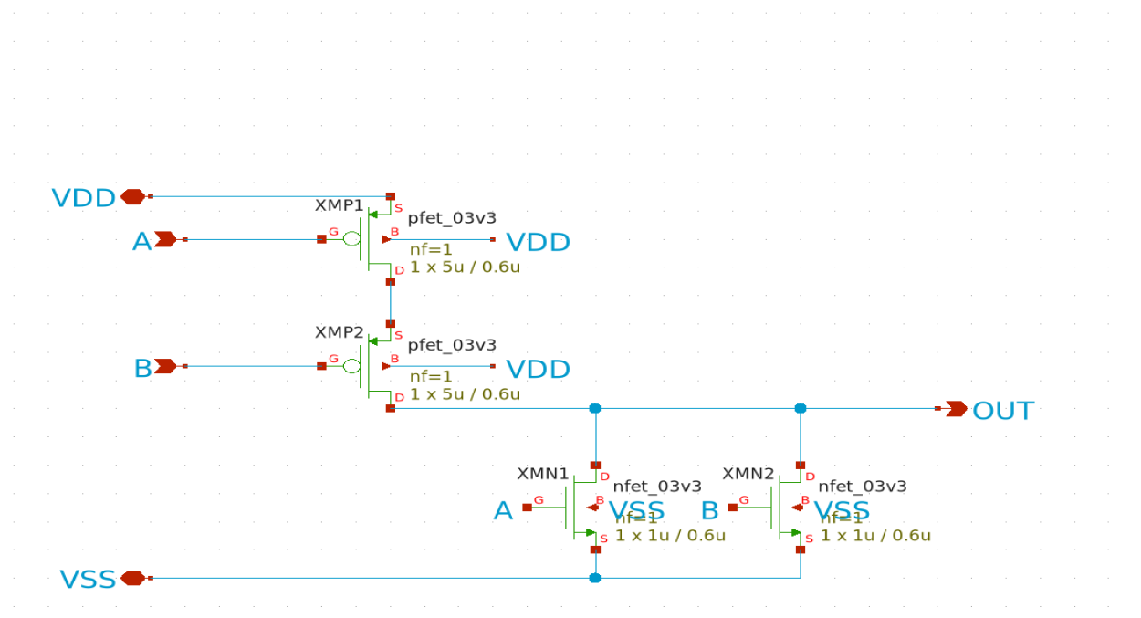
Pinout
Tile input pins mapped to NAND gate inputs:
| Tile pin | Cell pin |
|---|---|
ua\[4] |
A1 (Gate 1 input A; truth-table drive + HCT-window DC sweep) |
ui\_in\[1] |
B1 (Gate 1 input B) |
ui\_in\[2] |
A2 (Gate 2 input A) |
ui\_in\[3] |
B2 (Gate 2 input B) |
ui\_in\[4] |
A3 (Gate 3 input A) |
ui\_in\[5] |
B3 (Gate 3 input B) |
ui\_in\[6] |
A4 (Gate 4 input A) |
ui\_in\[7] |
B4 (Gate 4 input B) |
ui\_in\[0] |
unused |
Tile output pins mapped to NAND gate outputs:
| Tile pin | Cell pin |
|---|---|
ua\[0] |
Y1 (Gate 1 output) |
ua\[1] |
Y2 (Gate 2 output) |
ua\[2] |
Y3 (Gate 3 output) |
ua\[3] |
Y4 (Gate 4 output) |
Power pins: VDPWR is the 3.3 V supply, VGND is ground.
How to test
The procedure below is a basic functional verification of all four NAND gates.
-
Apply 3.3 V between
VDPWRandVGND. -
For each gate i, drive the two input pins to either 0 V or 3.3 V and read the corresponding output Y<sub>i</sub> on
ua\[i−1]:- Gate 1: A<sub>1</sub> on
ua\[4], B<sub>1</sub> onui\_in\[1] - Gate 2: A<sub>2</sub> on
ui\_in\[2], B<sub>2</sub> onui\_in\[3] - Gate 3: A<sub>3</sub> on
ui\_in\[4], B<sub>3</sub> onui\_in\[5] - Gate 4: A<sub>4</sub> on
ui\_in\[6], B<sub>4</sub> onui\_in\[7]
The output must follow the NAND truth table:
- Gate 1: A<sub>1</sub> on
| A | B | Y |
|---|---|---|
| 0 | 0 | 1 |
| 0 | 1 | 1 |
| 1 | 0 | 1 |
| 1 | 1 | 0 |
- HCT input-window check. Apply a slow DC ramp on
ua\[4]from 0 V to 3.3 V while holding B<sub>1</sub> (ui\_in\[1]) at 3.3 V. Observe Y<sub>1</sub> onua\[0]. The output must remain at logic high for V<sub>in</sub> ≤ 0.8 V and must be at logic low for V<sub>in</sub> ≥ 2.0 V.
External hardware
- 3.3 V DC power supply (≥ 50 mA capable).
- Digital multimeter for output-voltage measurement.
- (Optional) Variable low-voltage DC source for the HCT input-window check.
IO
| # | Input | Output | Bidirectional |
|---|---|---|---|
| 0 | |||
| 1 | B1 (Gate 1 input B) | ||
| 2 | A2 (Gate 2 input A) | ||
| 3 | B2 (Gate 2 input B) | ||
| 4 | A3 (Gate 3 input A) | ||
| 5 | B3 (Gate 3 input B) | ||
| 6 | A4 (Gate 4 input A) | ||
| 7 | B4 (Gate 4 input B) |
Analog pins
ua | PCB Pin | Internal index | Description |
|---|---|---|---|
| 0 | 21 | Y1 (Gate 1 output) | |
| 1 | 20 | Y2 (Gate 2 output) | |
| 2 | 17 | Y3 (Gate 3 output) | |
| 3 | 18 | Y4 (Gate 4 output) | |
| 4 | 19 | A1 (Gate 1 input A; 0/3.3 V for truth table, slow DC ramp 0->3.3 V for HCT window) |