292 3.3V Folded Cascode OTA
292 : 3.3V Folded Cascode OTA
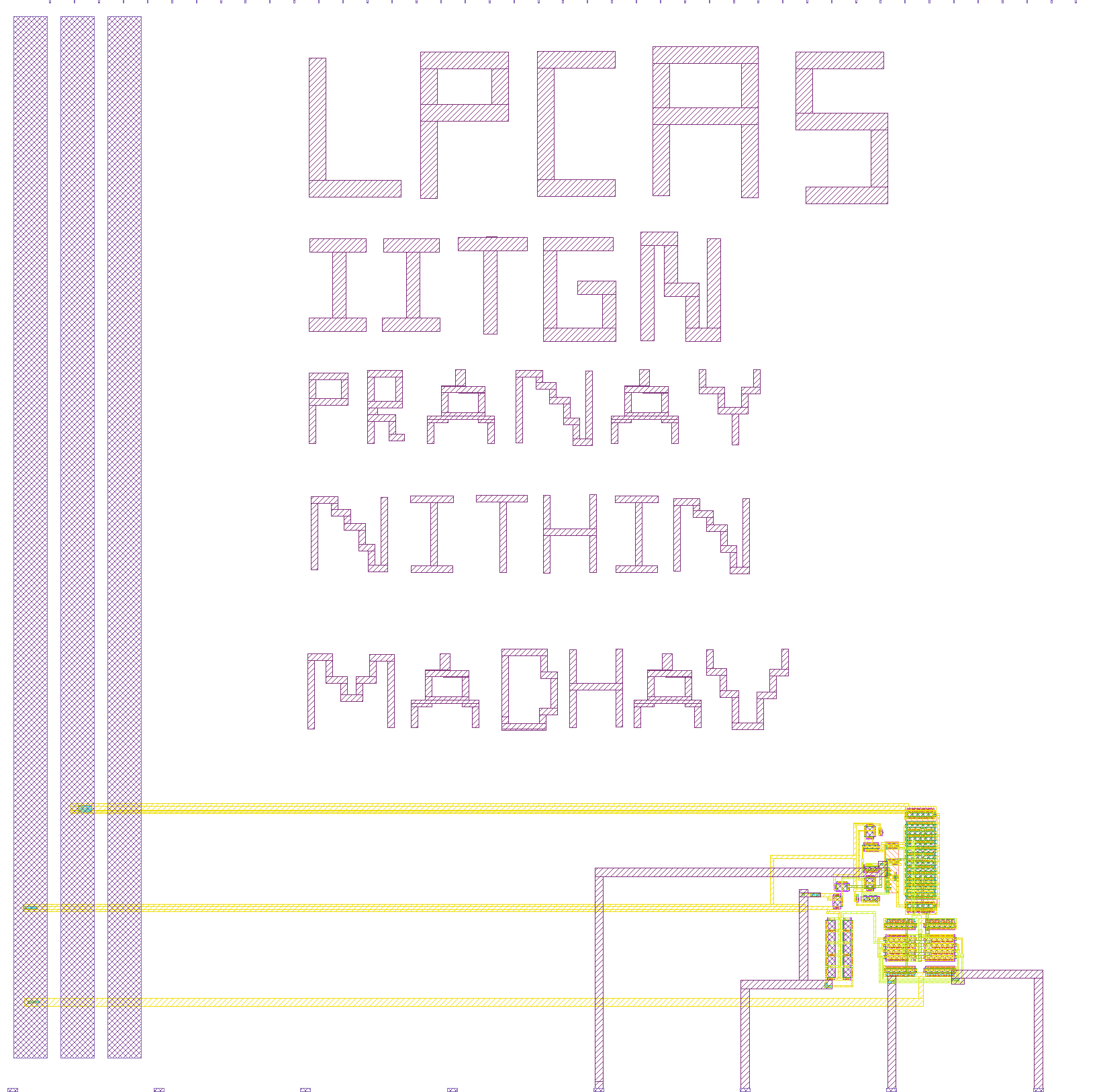
- Author: Pranay Arvind Patil and Nithin Purushothama
- Description: NMOS Input pair based Folded Cascode OTA
- GitHub repository
- Open in 3D viewer
- Open in Tiny Tapeout Explorer
- Clock: 0 Hz
TTGF0P3_LPCAS_FC_OTA
Overview
TTGF0P3_LPCAS_FC_OTA is a low-power Folded Cascode Operational Transconductance Amplifier (OTA) designed in the TTGF0P3 process. The amplifier is optimized for low-current operation while maintaining a large input common-mode range and output swing, making it suitable for a wide variety of analog signal-processing applications.
Key Features
- Folded Cascode architecture
- Low power consumption (~15 µA typical)
- Typical Unity Gain Bandwidth (UGB): ~100 kHz
- Wide input common-mode range
- Output swing approximately 0.5 V to 3.0 V
- Single-ended output
- Bias current programmable through external resistor
- Stable for capacitive loads up to approximately 50 pF
- Suitable building block for amplifiers, filters, DAC buffers, sensor interfaces, and analog computation blocks
Architecture and Circuit Operation
Folded Cascode Topology
The OTA uses a PMOS differential input pair combined with an NMOS folded-cascode structure.
Input Stage
The differential pair consists of:
- VINP (positive input)
- VINN (negative input)
The differential pair converts the input voltage difference into differential currents.
Advantages of using a PMOS input pair:
- Improved operation near ground
- Larger usable common-mode input range
- Lower flicker noise contribution
Folded Branch
The differential currents generated by the PMOS input pair are folded into NMOS devices.
This folded structure provides:
- High gain
- Increased output resistance
- Better headroom compared to telescopic cascode architectures
- Operation at relatively low supply voltages
The folded nodes transfer the signal current from the input stage into the output branch while preserving gain.
Cascode Gain Enhancement
Multiple cascode devices are used throughout the signal path.
Benefits include:
- Increased output resistance
- Increased intrinsic gain
- Better PSRR
- Improved isolation between stages
The gain enhancement is achieved without requiring additional gain stages, simplifying frequency compensation.
Current Mirror Load
The folded currents are mirrored and combined to produce a single-ended output at:
- VOUT
The current mirrors perform:
- Differential-to-single-ended conversion
- Gain generation
- Bias current distribution
Bias Network
The OTA uses an externally generated bias current.
The user must connect:
- A resistor between VDD and VBIAS
Recommended value:
- 2 MΩ
This resistor generates the reference current which is mirrored throughout the OTA.
Typical operating current:
- ~15 µA
Changing the resistor changes the OTA bias current:
| Bias Resistor | Approximate Effect |
|---|---|
| 2 MΩ | Nominal operation |
| 1 MΩ | Higher bias current |
| 500 kΩ | Maximum recommended bias current |
Increasing bias current generally results in:
- Higher bandwidth
- Higher slew rate
- Higher power consumption
Pin Description
| Pin | Name | Description |
|---|---|---|
| ua[0] | VINN | Inverting input |
| ua[1] | VINP | Non-inverting input |
| ua[2] | VBIAS | External bias resistor connection |
| ua[3] | VOUT | OTA output |
Power Supply
Recommended operating supply:
| Parameter | Value |
|---|---|
| VDD | 3.3 V |
| GND | 0 V |
Typical Connections
Biasing
Connect:
- 2 MΩ resistor between VDD and VBIAS
Example:
VDD
 |
[2 MΩ]
 |
VBIAS
Capacitive Load
Maximum recommended capacitive load:
- 50 pF
For characterization purposes:
- External capacitor ≈ 20 pF
- Probe/parasitics ≈ 30 pF
Total load:
CL ≈ 50 pF
Important Notes
Do NOT
- Short VOUT directly to GND
- Exceed recommended capacitive loading
- Leave VBIAS floating
- Apply input voltages outside supply rails
Recommended
- Set current limits on laboratory SMUs
- Start with a 2 MΩ bias resistor
- Verify supply current before performing measurements
Basic Functional Tests
1. Voltage Follower (Buffer)
Connect:
VINP = Input Signal
VINN = VOUT
Expected:
- Gain ≈ 1
- Demonstrates stability and bandwidth
2. Inverting Amplifier
Connect:
           Rf
VOUT <----/\/\----+
                  |
                  |
                 VINN
                  |
                 Rin
                  |
                VIN
Gain:
A_v = -Rf/Rin
3. Non-Inverting Amplifier
Gain:
A_v = 1 + Rf/Rg
Useful for:
- Sensor signal conditioning
- Analog front ends
4. Comparator Experiment
Operate OTA open-loop:
VINP > VINN  → VOUT rises
VINP < VINN  → VOUT falls
Useful for:
- Offset measurements
- Switching behavior characterization
Advanced Characterization Tests
5. Open-Loop Gain Measurement
Measure:
- DC gain
- Gain roll-off
- Dominant pole
Useful plots:
- Magnitude response
- Phase response
6. Unity-Gain Stability
Configure as a voltage follower.
Measure:
- Phase margin
- Settling time
- Ringing
7. Common-Mode Sweep
Sweep:
VINP = VINN
Measure:
- Input common-mode range
- Output swing limits
8. Output Swing Measurement
Sweep differential input slowly and record:
VOUT_MIN
VOUT_MAX
Expected output swing:
~0.5 V to ~3 V
9. Monte Carlo Analysis
Characterize:
- Offset voltage
- Gain variation
- GBW variation
- Bias current variation
Useful for mismatch verification.
10. Process Corner Verification
Run:
- TT
- FF
- SS
- FS
- SF
Verify:
- Gain
- UGB
- Phase Margin
- Current Consumption
11. Temperature Sweep
Recommended:
-40°C
25°C
85°C
125°C
Measure:
- Offset drift
- Gain drift
- Bandwidth variation
12. PSRR Measurement
Inject ripple into:
- VDD
Measure:
PSRR+ = ΔVDD / ΔVOUT
Useful plots:
- PSRR vs Frequency
13. CMRR Measurement
Apply common-mode excitation:
VINP = VINN
Measure:
- Common-mode gain
- Differential gain
Compute:
CMRR = Ad / Acm
14. Noise Analysis
Measure:
- Input referred noise
- Output noise density
- Integrated RMS noise
Useful for sensor applications.
Practical Application Examples
This OTA can be used as the active element in many analog circuits.
Filters
Active Low-Pass Filter
Applications:
- Sensor conditioning
- Audio filtering
- Anti-aliasing
Active High-Pass Filter
Applications:
- DC removal
- AC coupling
Band-Pass Filter
Applications:
- Communication systems
- Tone detection
State Variable Filter
Applications:
- Analog signal processing
- Tunable filtering
Data Converters
R-2R DAC Buffer
Use the OTA as:
- Output buffer
- Reconstruction amplifier
Benefits:
- High input impedance
- Improved DAC drive capability
SAR ADC Front-End Buffer
Applications:
- Sample-and-hold driving
- Capacitive DAC buffering
Sensor Interfaces
Suitable for:
- Temperature sensors
- Resistive sensors
- Photodiodes
- Capacitive sensing systems
Signal Conditioning
Applications:
- Instrumentation amplifiers
- Differential-to-single-ended conversion
- Analog preprocessing
Peak Detector
Build:
- Precision peak detector
- Envelope detector
Applications:
- AM demodulation
- Signal monitoring
Integrator
Applications:
- Analog computation
- PID controllers
- Sigma-delta loops
Differentiator
Applications:
- Edge detection
- High-frequency enhancement
Oscillator Building Block
Can be used in:
- Wien bridge oscillators
- Quadrature oscillators
- Relaxation oscillators
Current-to-Voltage Converter
Useful for:
- Photodiodes
- Current-output sensors
- Electrochemical sensors
Suggested Characterization Results to Include
The following plots are highly recommended for documentation:
DC Characterization
- Transfer curve
- Input common-mode sweep
- Output swing plot
AC Characterization
- Open-loop gain
- UGB
- Phase margin
Transient Characterization
- Step response
- Settling behavior
- Slew rate
Statistical Verification
- Monte Carlo offset histogram
- Gain distribution
- Current distribution
PVT Verification
- Corner sweeps
- Temperature sweeps
Supply Rejection
- PSRR vs frequency
Common Mode Performance
- CMRR vs frequency
Noise
- Input referred noise
- Output noise density
Typical Operating Conditions
| Parameter | Typical Value |
|---|---|
| Supply Voltage | 3.3 V |
| Bias Resistor | 2 MΩ |
| Current Consumption | ~15 µA |
| Capacitive Load | ≤ 50 pF |
| Output Swing | ~0.5 V to 3.0 V |
| Topology | Folded Cascode OTA |
| Output Type | Single Ended |
| UGB | ~100 kHz |
Authors
- Nithin P
- Pranay Patil
- LPCAS Group, IIT Gandhinagar
This OTA is intended as a reusable low-power analog building block for educational, research, and mixed-signal integrated circuit design projects.
IO
| # | Input | Output | Bidirectional |
|---|---|---|---|
| 0 | |||
| 1 | |||
| 2 | |||
| 3 | |||
| 4 | |||
| 5 | |||
| 6 | |||
| 7 |
Analog pins
ua | PCB Pin | Internal index | Description |
|---|---|---|---|
| 0 | 12 | VINN | |
| 1 | 13 | VINP | |
| 2 | 14 | VBIAS | |
| 3 | 15 | VOUT |