256 256x8 SRAM
256 : 256x8 SRAM
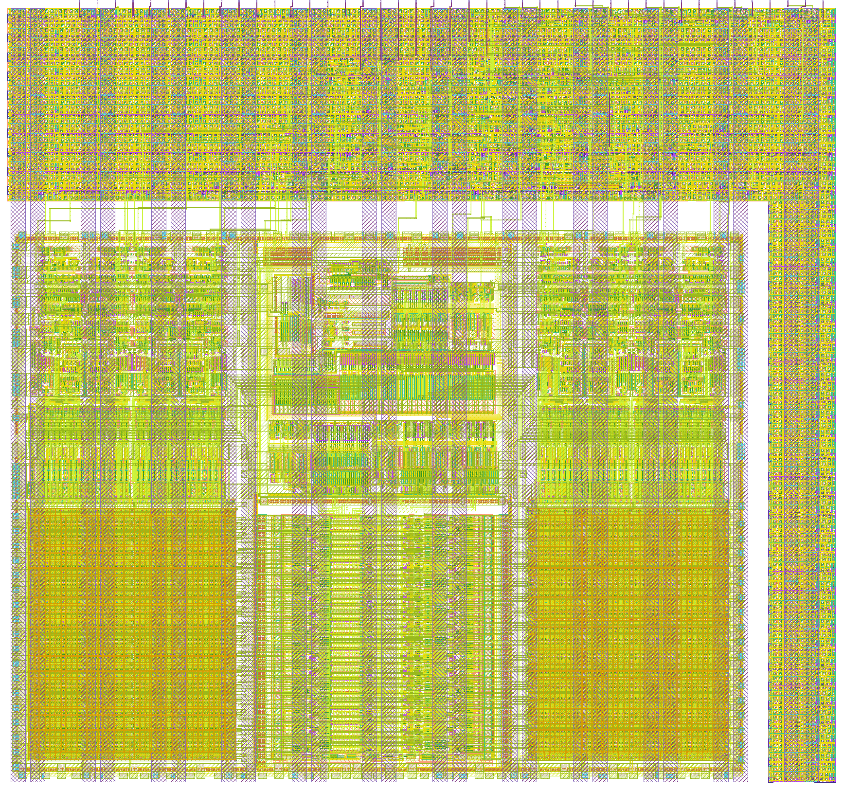
- Author: Julia Desmazes
- Description: 256x8 SRAM for testing
- GitHub repository
- Open in 3D viewer
- Open in Tiny Tapeout Explorer
- Clock: 50000000 Hz
Open Circuit Design 256x8 SRAM for gf180 test.
How it works
SRAM is entirely cleared on reset.
Although this is technically an 256x8 SRAM only the top 128 entries are addressable.
There are 6 bits of address, 8 bits of input data and 8 bits of output data.
De-assert gwen to write, else SRAM will be in read mode.
Beware, incomming data/write enable/address are flopped once before the SRAM and outgoing data is also flopped once
before reaching the uo_out pins.
Pinout
From SRAM documentation:
| Signal | Direction | Description |
|---|---|---|
| CLK | Input | Clock for the memory. Rising edge triggers operation. All inputs are latched at rising edge of the clock signal. |
| CEN | Input | Memory Enable, Active Low. When CEN is Low, the memory is enabled. When CEN input is High, the memory is deactivated but internal states are retained. CEN must be high before 1st running cycle. |
| A[7:0] | Input | Address Input. This Address input port is used to address the location to be written during the write cycle and read during the read cycle. |
| GWEN | Input | Write Enable Input. The RAM is in write cycle when GWEN is low. The RAM is in read cycle when GWEN is high. |
| WEN[7:0] | Input | Bit Write Mask, Active Low. When the memory is in the write cycle, selectively write into individual outputs are controlled by WEN[7:0]. For example, if CEN, GWEN, WEN[0] are low and WEN[7:1] are high, only D[0] will write into the addressed location and D[7:1] will be ignored during CLK low to high transition. |
| D[7:0] | Input | Data input bus. The data input bus is used to write data into the memory location specified by address input port during the write cycle. |
| Q[7:0] | Output | Data output bus. It outputs the contents of the memory location addressed by the Address Input signals. |
| VDD | Power | Power pin. |
| VSS | Ground | Ground pin. |
How to test
See above.
External hardware
None
IO
| # | Input | Output | Bidirectional |
|---|---|---|---|
| 0 | addr[0] | data_rd[0] | data_wr[0] |
| 1 | addr[1] | data_rd[1] | data_wr[1] |
| 2 | addr[2] | data_rd[2] | data_wr[2] |
| 3 | addr[3] | data_rd[3] | data_wr[3] |
| 4 | addr[4] | data_rd[4] | data_wr[4] |
| 5 | addr[5] | data_rd[5] | data_wr[5] |
| 6 | addr[6] | data_rd[6] | data_wr[6] |
| 7 | gwen | data_rd[7] | data_wr[7] |