294 Oscillating Bones
294 : Oscillating Bones
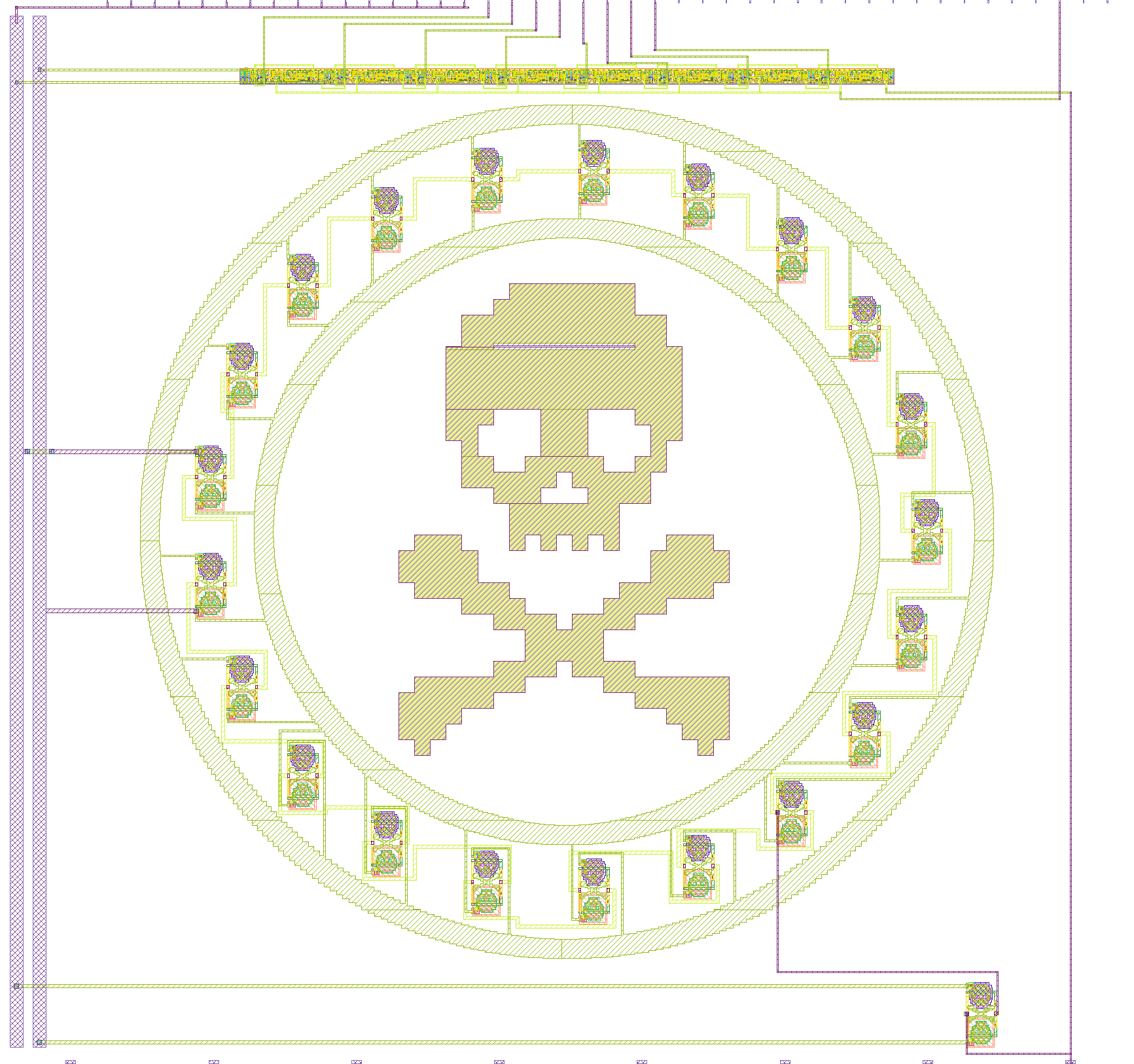
- Author: Uri Shaked
- Description: A stylish SkullFET ring oscillator (~120 MHz) with an 8-bit /2../256 divider
- GitHub repository
- Open in 3D viewer
- Open in Tiny Tapeout Explorer
- Clock: 0 Hz
How it works
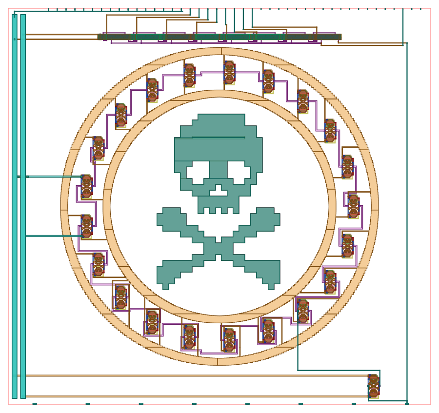
A stylish ring oscillator built from SkullFET transistors — MOSFETs hand-drawn in the shape
of skulls. A chain of 21 SkullFET inverters forms a ring oscillator that generates a ~120 MHz
square wave; an 8-bit ripple divider then produces /2 through /256 taps on uo_out[0..7]. The
raw oscillation is brought out on the analog pin ua[0] through one more SkullFET wired as a
buffer, so an external probe/load on ua[0] can't pull the ring frequency.
This is the gf180mcu (GlobalFoundries 180nm) port of the design, migrated from the original
IHP sg13g2 version. The SkullFETs are 3.3V devices running directly on the 3.3V core supply
(VDPWR). The skull artwork is preserved verbatim from the original; only the layer stack, device
implants and feature sizes were retargeted to gf180mcuD (a uniform 1.45× scale clears the 180nm
width/spacing/gate rules; grid-snap, exact-cut and metal-slot passes then make it KLayout
sign-off-clean — see scripts/remap_to_gf180.py).
| Pin | Signal | Post-layout frequency |
|---|---|---|
| ua[0] | osc_out (buffered raw 3.3V oscillation) | ~120 MHz |
| uo_out[0] | osc_div_2 | ~60 MHz |
| uo_out[1] | osc_div_4 | ~30 MHz |
| uo_out[2] | osc_div_8 | ~15 MHz |
| uo_out[3] | osc_div_16 | ~7.5 MHz |
| uo_out[4] | osc_div_32 | ~3.7 MHz |
| uo_out[5] | osc_div_64 | ~1.9 MHz |
| uo_out[6] | osc_div_128 | ~0.94 MHz |
| uo_out[7] | osc_div_256 | ~0.47 MHz |
(uo_out[0] is the LSB / ÷2, uo_out[7] the MSB / ÷256.) All unused outputs — uio_out[7:0] and
the output-enables uio_oe[7:0] — are tied low in the macro, so the bidirectional pads stay in
input mode.
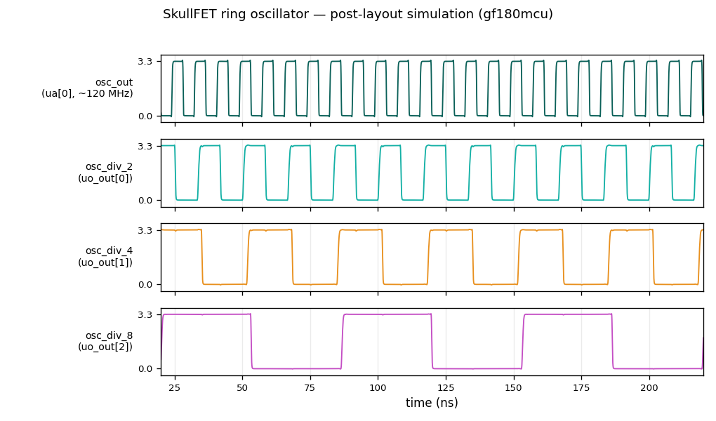
Post-layout simulation (extract the hardened GDS with magic, simulate with the gf180mcuD
ngspice models — run make sim): the ring oscillates rail-to-rail at ~120 MHz and the 8-stage
divider produces clean /2 .. /256 taps. The testbench supplies only VDPWR/VGND and the substrate
bias — it does not force any std-cell rail or device well, so the result reflects the actual
extracted connectivity (every pfet body is tied to VDPWR through its n-well tap, every std-cell rail
is strapped to VDPWR/VGND — nothing floats). With the buffer, a swept capacitive load on ua[0]
(0→10 pF) leaves the ring frequency unchanged at ~120 MHz; without it the same load would drop
the ring 25–60 %.
Simulation results
osc_out (the buffered ~120 MHz oscillation on ua[0]) and the first three divider taps, captured
from the post-layout netlist (make plot):
Reset
rst_n (active-low) resets only the divider — it asynchronously clears all eight flip-flops,
so while rst_n is held low the divided taps uo_out[0..7] sit at 0. The 21-stage ring oscillator
has no reset and free-runs whenever the design is powered, so ua[0] keeps oscillating at full
speed even during reset. Release rst_n (high) and the divider starts counting from a known phase.
clk and ena are not used — the ring self-clocks the divider.
How to test
Connect an oscilloscope to a low divider tap such as uo_out[7] (÷256, ~0.5 MHz) or
uo_out[4] (÷32, ~3.7 MHz) — scope-friendly. The fast taps and the buffered ua[0] (~120 MHz)
exceed typical GPIO bandwidth, so the analog pin ua[0] is the place to look for the raw
oscillation. Note that uo_out[0..7] stay at 0 until you release rst_n.
External hardware
None — just an oscilloscope.
IO
| # | Input | Output | Bidirectional |
|---|---|---|---|
| 0 | osc_div_2 | ||
| 1 | osc_div_4 | ||
| 2 | osc_div_8 | ||
| 3 | osc_div_16 | ||
| 4 | osc_div_32 | ||
| 5 | osc_div_64 | ||
| 6 | osc_div_128 | ||
| 7 | osc_div_256 |
Analog pins
ua | PCB Pin | Internal index | Description |
|---|---|---|---|
| 0 | 14 | osc_out |