202 Crazy logic gates
202 : Crazy logic gates
- Author: Fatemeh & Yaning
- Description: The craziest logic gates ever made
- GitHub repository
- Open in 3D viewer
- View in Wokwi
- Clock: 10000 Hz
How it works
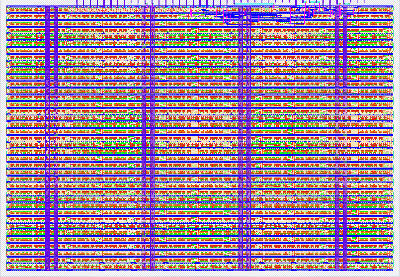
It is super complicated, even I don't know. It's just a bunch of gates that are thrown together to see how they will react with each other. A fun experiment.
How to test
Just hook it up to a seven-segment or an LED bar so see if it works or not. When everything is off the seven-segment should show 4.
External hardware
DIP switch, resistors, and LED bar graph/seven-segment display.
IO
| # | Input | Output | Bidirectional |
|---|---|---|---|
| 0 | input a | output a AND b | |
| 1 | input b | output NOT | |
| 2 | input c | output XNOR | |
| 3 | input d | output MUX | |
| 4 | input e | output OR | |
| 5 | input f | output NAND | |
| 6 | input g | output NOR | |
| 7 | input h | output XOR |