34 Dickson Charge Pump

34 : Dickson Charge Pump
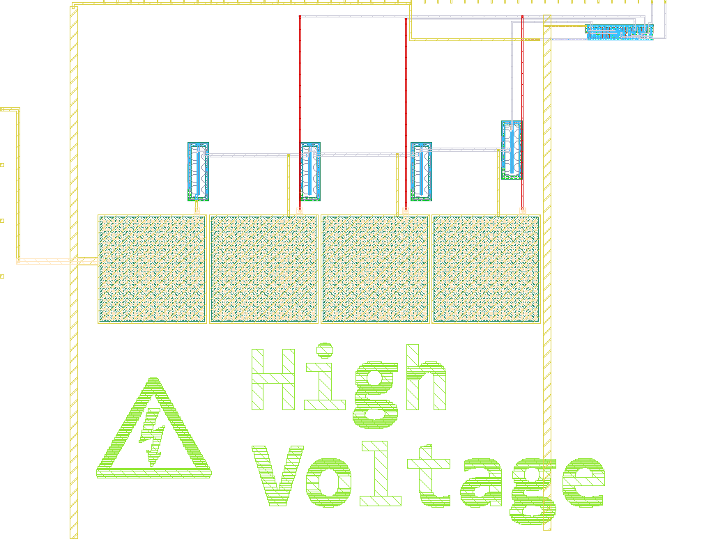
Design render

How it works

A 3-stage dickson charge pump.

How to test

Apply a clock signal of 2 MHz to the clk input. You should see the output voltage on the ua[0] (vout) pin rise to ~3.2 V.

Layout
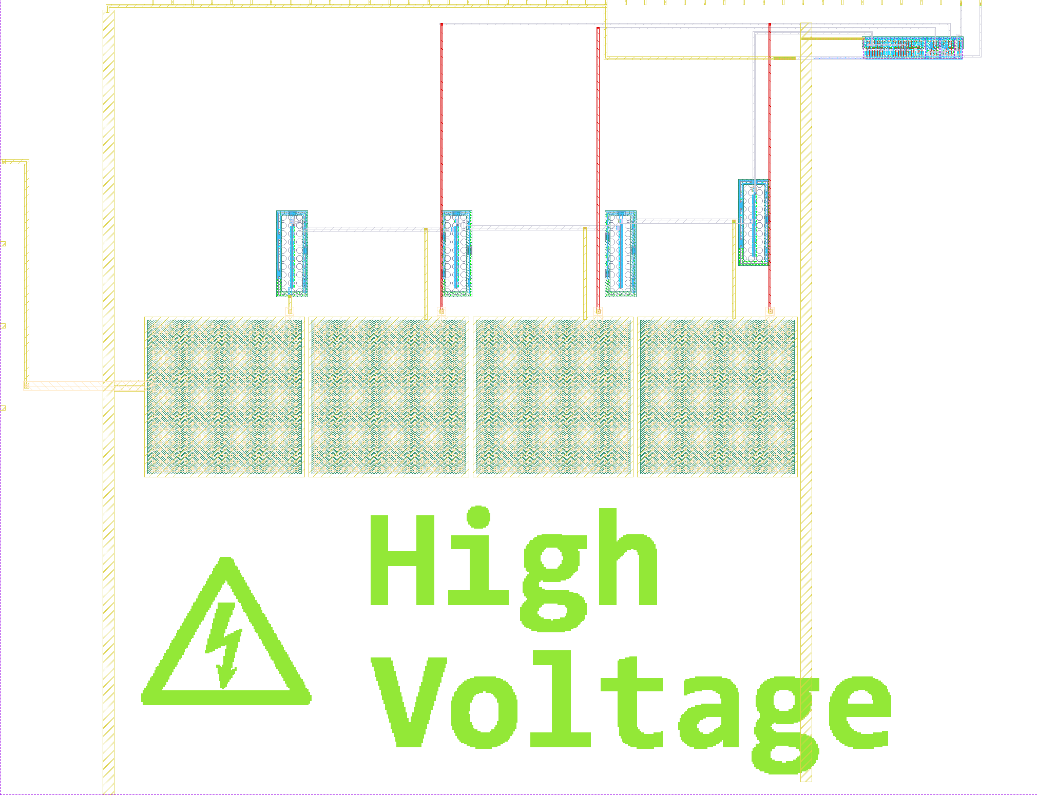
layout.png

Post layout simulation results

Tested with 2 MHz input clock and 7 Mega Ohm load.
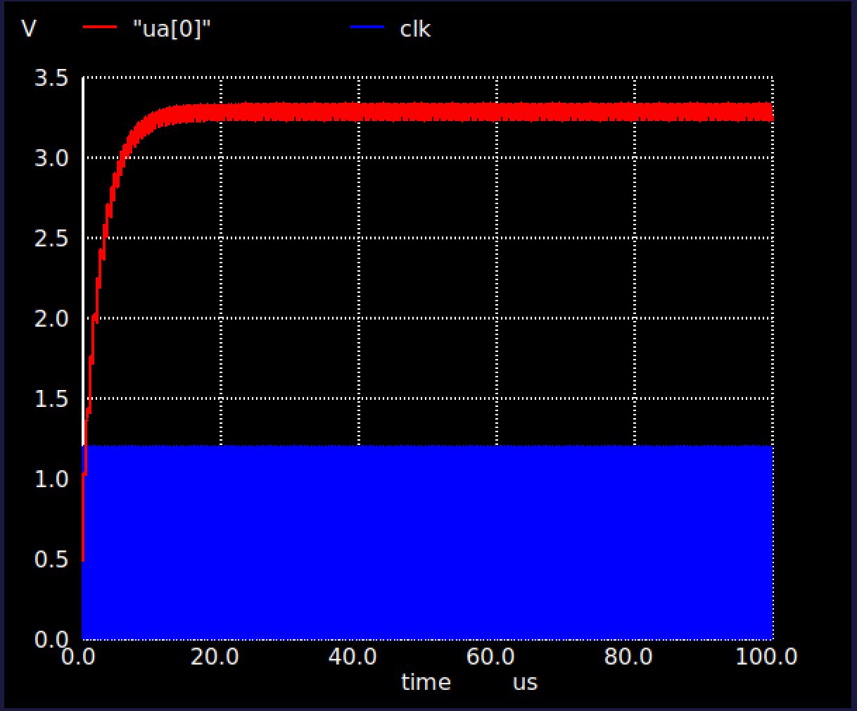
post_layout_sim.png

IO

#InputOutputBidirectional
0
1
2
3
4
5
6
7

Chip location

Controller Mux Mux Mux Mux Mux Mux Mux Mux tt_um_chip_rom (Chip ROM) tt_um_factory_test (Tiny Tapeout Factory Test) tt_um_htfab_r2r_dac (R-2R DAC) tt_um_algofoogle_antonalog (Antonalog analog VGA) tt_um_NicklausThompson_555_1x1 (HBT Comparator) tt_um_urish_dickson_pump (Dickson Charge Pump) tt_um_htfab_yadge (Yet Another Diffraction Grating Experiment) tt_um_colorful_stripes (Colorful stripes) tt_um_rte_eink_driver (E-ink display driver) tt_um_bleeptrack_prism (Prism) tt_um_calonso88_spi_test (SPI test) tt_um_sathworld_spi_pwm_peripheral (SPI-connected PWM generator) tt_um_lfsr_stevej (Linear Feedback Shift Register) tt_um_strau0106_simple_viii (simple-viii) tt_um_algofoogle_ro_worker (Ring Oscillator Worker) tt_um_vga_clock (VGA clock) tt_um_a1k0n_demo (Demo by a1k0n) tt_um_algofoogle_fun_vga_clock (Fun VGA Clock) tt_um_digital_clock_example (7-Segment Digital Desk Clock) tt_um_urish_simon (Simon Says memory game) tt_um_ihp_logo_screensaver (VGA Screensaver with the IHP Logo) tt_um_zerotoasic_logo_screensaver (VGA Screensaver with Zero to ASIC Logo) tt_um_arud4172_ROOTS_vga (ROOTS logo vga) Available