490 Time Domain ADC
490 : Time Domain ADC
- Author: M. Taufiqul Huda
- Description: Time Domain Comparator Based ADC
- GitHub repository
- Open in 3D viewer
- Clock: 1000000 Hz
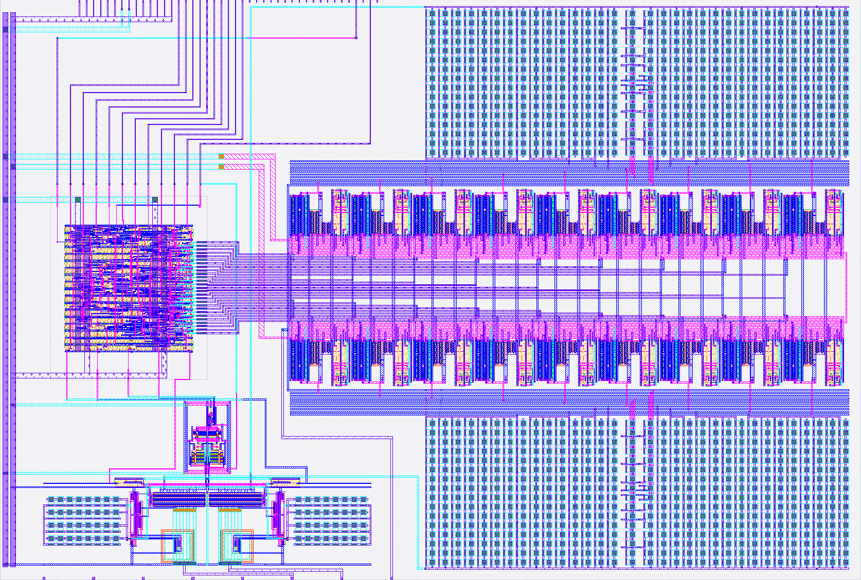
Low-Power SAR-ADC for PPG Signal Acquisition
This repository contains the design files and simulation results for a 10-bit SAR-ADC in 180nm CMOS, optimized for low-power biomedical applications like Photoplethysmogram (PPG) signal acquisition.
Project Overview
The primary goal of this project is to design an efficient and accurate ADC for low-power wearable devices. The design focuses on a 10-bit monotonic SAR-ADC architecture utilizing a time-domain comparator to achieve power consumption in the microwatt range.
The final post-layout design is ready for fabrication, achieving a power consumption of 23.25 µW and an Effective Number of Bits (ENOB) of 6.44 bits. The design has been verified to accurately acquire PPG signals, making it suitable for biomedical applications.
Key Specifications
The final specifications from the post-layout simulation are as follows:
| Parameter | Tipikal | Unit |
|---|---|---|
| Technology | CMOS 180nm | - |
| Supply Voltage | 1.80 | V |
| Resolution | 10 | bits |
| Input Voltage Range | 0 - 1.8 | V |
| Conversion Time | 5.2 | µs |
| Power Consumption | 23.25 | µW |
| ENOB | 6.44 | bits |
| SNR | 41.03 | dB |
| THD | -50.11 | dB |
| INL | -3 / +3 | LSB |
| DNL | -1 / +4 | LSB |
Architecture Details
The design is based on the Monotonic Switching SAR-ADC architecture, which is known for its power efficiency and smaller capacitor array requirements.
The core innovation lies in the Time Domain Comparator, which is based on a Voltage-Controlled Delay Line (VCDL). This approach significantly reduces power consumption compared to traditional dynamic comparators.
Key Components:
- Track/Hold (T/H) Switch: A Bootstrapped Switch for input signal sampling.
- Capacitive DAC (CDAC): Generates the reference voltage for comparison.
- Time Domain Comparator: The low-power VCDL-based comparator.
- SAR Logic: Controls the successive approximation algorithm.
✍️ How to Cite
If you use this design or information from this project, please cite the original proceedings:
M. T. Huda, A. N. Irfansyah, and Tasripan, "Desain SAR-ADC Berbasis Time Domain Comparator Rendah Daya Untuk Perekaman Sinyal Photoplethysmogram Menggunakan Teknologi CMOS," Departemen Teknik Elektro, Institut Teknologi Sepuluh Nopember, Surabaya, 2025.
Resources
This project is based on the research and findings presented in the paper above. For further technical details on the implementation and simulation results, please refer to the full document.
IO
| # | Input | Output | Bidirectional |
|---|---|---|---|
| 0 | EN | CKO | DATA[1] |
| 1 | DATA[8] | DATA[0] | |
| 2 | DATA[7] | ||
| 3 | DATA[6] | ||
| 4 | DATA[5] | ||
| 5 | DATA[4] | ||
| 6 | DATA[3] | ||
| 7 | DATA[2] |
Analog pins
ua | PCB Pin | Internal index | Description |
|---|---|---|---|
| 0 | A1 | 1 | VCM |
| 1 | A3 | 3 | VIN |
| 2 | A2 | 2 | VIP |