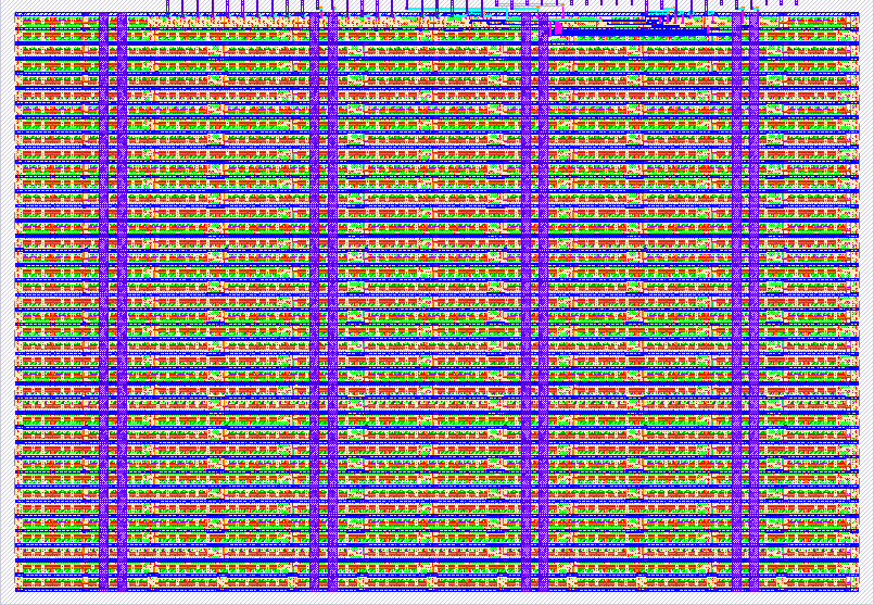
811 Tiny Tapeout Test Gates
811 : Tiny Tapeout Test Gates

- Author: Mobin Alimohammadi
- Description: Demo for logic gates and a clock divider
- GitHub repository
- Open in 3D viewer
- View in Wokwi
- Clock: 10000 Hz
How it works
AND, NAND gates connected to input a and b.
NOT gate connected to input d.
Two NOR gates connected in series with one feedback loop from output 7 and inputs from g and h.
Logic behavior
AND gate: Y_AND = a · b
NAND gate: Y_NAND = ¬(a · b)
NOT gate: Y_NOTd = ¬d
NOR latch: Inputs: g → Set (S), h → Reset (R) Outputs: Q (main), Q̅ (complement) Characteristic equations: Q = NOR(R, Q̅) Q̅ = NOR(S, Q)
| a | b | d | Y_AND | Y_NAND | Y_NOTd |
|---|---|---|---|---|---|
| 0 | 0 | 0 | 0 | 1 | 1 |
| 0 | 0 | 1 | 0 | 1 | 0 |
| 0 | 1 | 0 | 0 | 1 | 1 |
| 0 | 1 | 1 | 0 | 1 | 0 |
| 1 | 0 | 0 | 0 | 1 | 1 |
| 1 | 0 | 1 | 0 | 1 | 0 |
| 1 | 1 | 0 | 1 | 0 | 1 |
| 1 | 1 | 1 | 1 | 0 | 0 |
SR latch (g → S, h → R)
| S (g) | R (h) | Q_next | Q̅_next | Description |
|---|---|---|---|---|
| 0 | 0 | Q_prev | ¬Q_prev | Hold (no change) |
| 1 | 0 | 1 | 0 | Set |
| 0 | 1 | 0 | 1 | Reset |
| 1 | 1 | X | X | Forbidden / Undefined |
How to test
Power & setup Connect all inputs to VCC or GND through pull-up/pull-down resistors. Use pushbuttons or switches for a, b, d, g, and h. Verify basic gates Toggle a and b to confirm AND/NAND output behavior. Toggle d to confirm the NOT gate output. Test the SR latch With g=0, h=0, the latch should hold its previous state. With g=1, h=0, it sets Q=1. With g=0, h=1, it resets Q=0. Avoid g=1, h=1 (undefined state).
Observe outputs Use LEDs or a 7-segment display to visualize logic states. Q may drive one LED; Y_AND, Y_NAND, Y_NOTd can drive others.
External hardware
Momentary pushbuttons for inputs (a, b, d, g, h) Pull-up resistors (10 kΩ typical) LEDs or a 7-segment display for output indication Breadboard, jumper wires, regulated VCC supply
IO
| # | Input | Output | Bidirectional |
|---|---|---|---|
| 0 | input a | output and | |
| 1 | input b | output nand | |
| 2 | input c | output not | |
| 3 | input d | output not | |
| 4 | input e | output | |
| 5 | input f | output | |
| 6 | input g | output | |
| 7 | input h | output nor feedback |