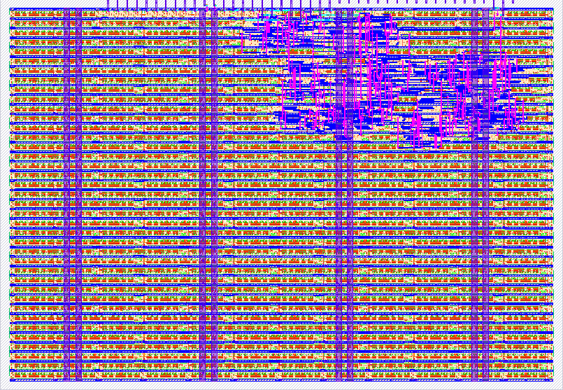
421 Demux
421 : Demux

- Author: Andrey Shornikov
- Description: ASIC controls ADG732 multiplexer chip switching its input to one of 25 output channels each second
- GitHub repository
- Open in 3D viewer
- Clock: 10000000 Hz
How it works
This project is originally to test multistrand cable asseblies for proper connection - applying voltage to one pin and at the end visualizing that at the other end of multistage cable assembly correct, one and only one LED lights up. Therefore it iterates single voltage input through multiple outputs, using 32-channel multiplexer chip ADG732 with a human-comfortable switching time around 1 second.
The ASIC contains a clock divider to divide 10 MHz clock to 1 Hz. On each divided cycle it increments 5-bit adddress of output channel on the ADG732 chip and generates chip select (cs) and write (wr) signals for ADG732. WR signal makes ADG732 to read and use new output channel from the 5-bit address bus.
How to test
Verilog can be tested with FPGA like iCE40. There are two options use the output as is for ADG732, or use with a LED PMOD (which needs inverted signals). The second option uses an inverter top module, that is not included in this project, but is available in the repository for the demux itself - https://github.com/AndyShor/fpga_demux
Testing with actual ADG732 requires chip (about 10$) and a custom made PCB to interface. I designed a basic PCB, files soon will be added to fpga_demux repo.
External hardware
For FPGA tests I used - ice sugar nano board (https://github.com/wuxx/icesugar-nano) with ice40 FPGA LP1K and CM36 package type, and inverting PMOD LED module supplied with it.
For tests with actual chip I used ADG732BSUZ chip on a custom PCB I ordered from JLCPCB.
IO
| # | Input | Output | Bidirectional |
|---|---|---|---|
| 0 | demux_ena | ||
| 1 | wr | ||
| 2 | cs | ||
| 3 | set_ch[0] | ||
| 4 | set_ch[1] | ||
| 5 | set_ch[2] | ||
| 6 | set_ch[3] | ||
| 7 | set_ch[4] |