196 TTSKY25A Register File Test
196 : TTSKY25A Register File Test
- Author: Sylvain Munaut
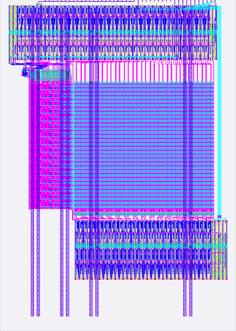
- Description: Test structures for a future register file macro
- GitHub repository
- Open in 3D viewer
- Clock: 0 Hz
- Feedback: ✅ 1
How it works
It's basically a SRAM with 1 write port and 2 read ports. See design data for information
How to test
No test procedure has been written yet and it's not meant to be tested by the "demo board" but instead on a dedicated test platform.
External hardware
To do any meaningful timing testing you'll need some FPGA hardware to drive the various control signal in sequence with precise timings.
The exact testing platform is still TBD.
IO
| # | Input | Output | Bidirectional |
|---|---|---|---|
| 0 | tbd | tbd | tbd |
| 1 | tbd | tbd | tbd |
| 2 | tbd | tbd | tbd |
| 3 | tbd | tbd | tbd |
| 4 | tbd | tbd | tbd |
| 5 | tbd | tbd | tbd |
| 6 | tbd | tbd | tbd |
| 7 | tbd | tbd | tbd |
User feedback
- smunaut👑: Seems to work fine. Executed a memory test with tens of thousands of random R/W cycles and all results were expected. Timing is not characterized yet, rpi pico isn't good enough, will need a FPGA to control things more tightly. But a very good start !!! ( Note this is _not_ the final version of the macro on this shuttle, this only tests the bit-cell and address decoders ).