520 Programmable threshold voltage sensor
520 : Programmable threshold voltage sensor
- Author: Andrea Possemato - Mattia A. Di Nicola
- Description: voltage sensor with 3 bit (8 voltage levels) threshold selector
- GitHub repository
- Open in 3D viewer
- Clock: 0 Hz
How it works
This programmable threshold voltage comparator allows comparing a voltage provided externally by the user (Vref signal) with a voltage level (threshold). The threshold voltage selection is controlled by 3 digital signals (in[0], in[1] and in[2] signals), which allow selecting one of the 8 possible threshold voltage levels. 7 of these levels are fixed (from 001 to 111 code), and only one (000 code) can be set by the user (in0 signal).
The output voltage (out signal) will be high (1.8V) when the selected threshold voltage is lower than Vref (Vth < Vref); otherwise, it will be low (0V).
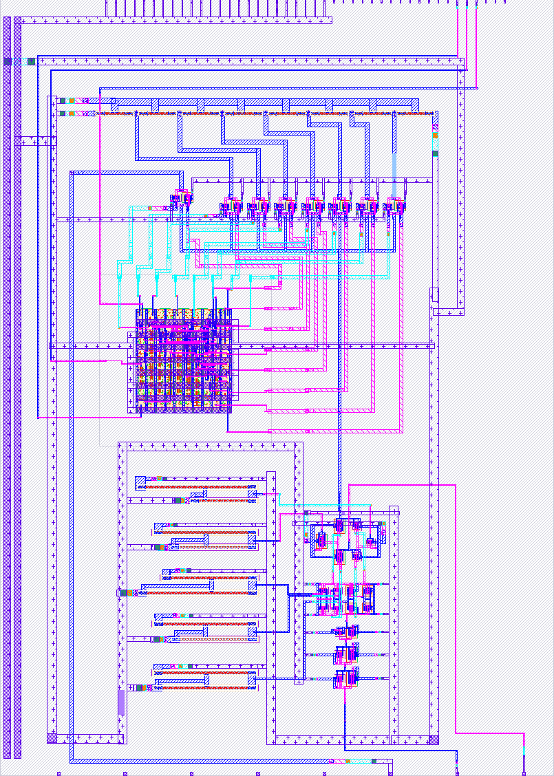
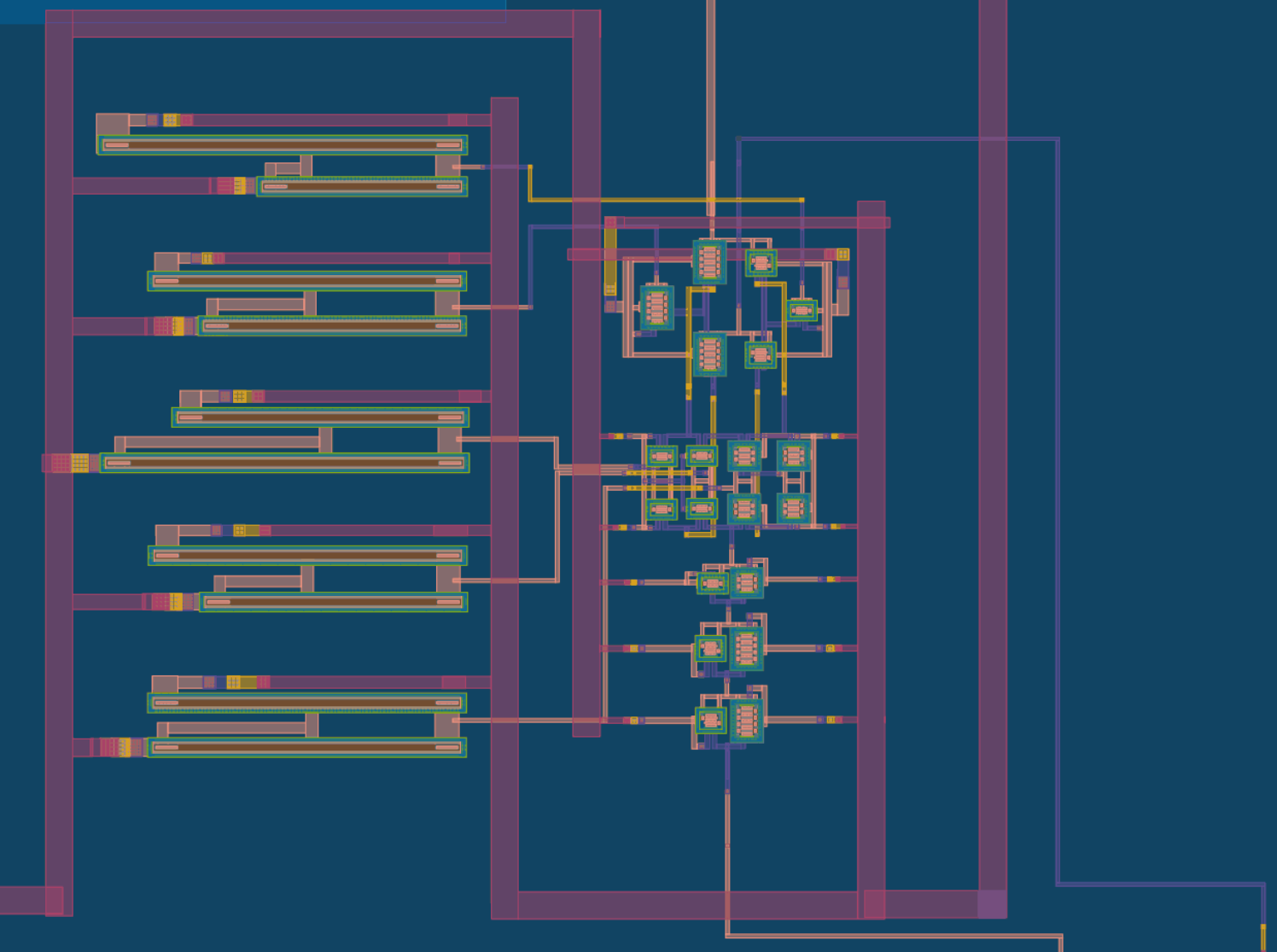
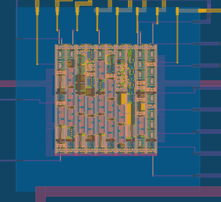
The image below gives a simple overview of the entire project.
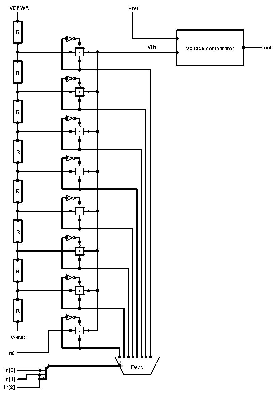
We can see all used components. We have 8 equal resistors whom provide fixed thresholds for 7 passgates. The one at the bottom is linked to external pin in0 for free user voltage threshold. Every passgate is built using Pmos and Nmos both. Every passgate's gates are linked to decoder, who provides direct and negative signal to enable or disable each passgate.
Values of resistance and fixed voltage thresholds can be read opening xschem/analog.sch file with xschem.
The next section explains how Voltage comparator is made.
Voltage comparator
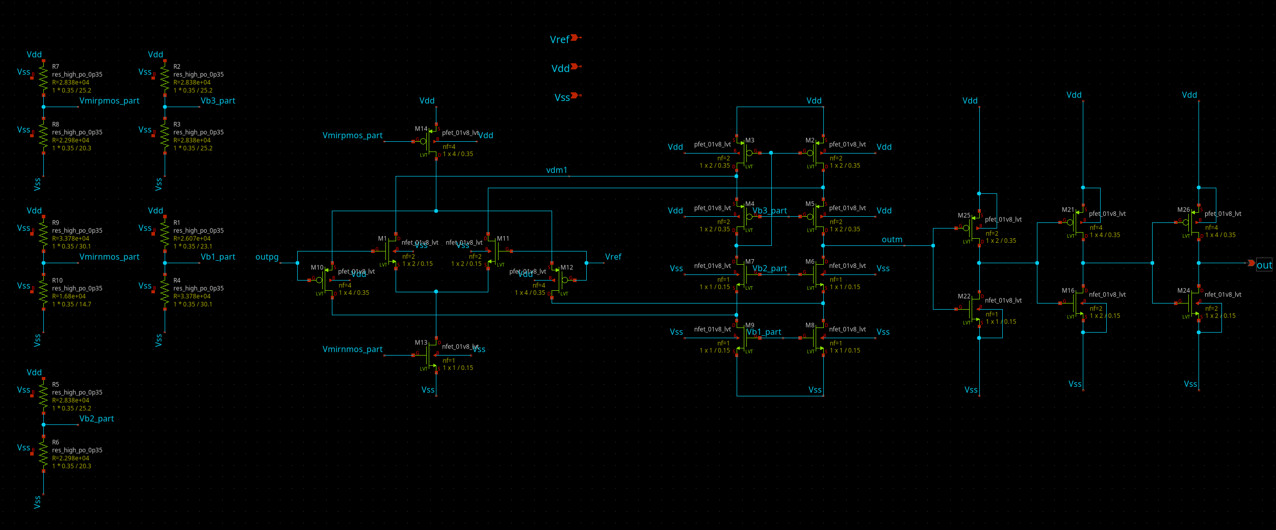
Compare inputs between 0 and 1.8 V on both Vref and outpg. The output goes to 1.8 V (logic 1) if Vref > outpg; otherwise, it goes to 0 V (logic 0).
| Min | Max | 1 logic | 0 logic | |
|---|---|---|---|---|
| Output current | - | 150μA | - | - |
| Vref | 0V | 1.8V | - | - |
| outpg | 0V | 1.8V | - | - |
| out | 0V | 1.8V | - | - |
| Zout | - | - | ~ 11.5KΩ | ~ 2.8KΩ |
Decoder 3 to 8
In verilog/rtl folder you can find the verilog file used to generate gds/decoder_p.gds and gate level verilog file (in gl folder). Note that hardening process (who creates .gds and GL file) was made using commands of MakeFile contained in Matt Venn's R2R DAC example's (https://github.com/mattvenn/tt06-analog-r2r-dac).
Performance
Rise time of out signal (from 0.2V to 1.6V) is 8.5ns.
Fall time of out signal (from 1.6V to 0.2V) is 19ns.
Maximum switching frequency of all input signals (even if they switch all at the same time) is 100KHz, i.e. all signals can switch at the same time, but the fastest one MUST NOT exced 100KHz.
| Min | Max | Typical | |
|---|---|---|---|
| VDPWR | - | - | 1.8V |
| VGND | - | - | 0V |
| Vref | 0V | 1.8V | - |
| in0 | 0V | 1.8V | - |
| Switching frequency (all inputs) | - | 100KHz | - |
| Rise time | - | - | 8.5ns |
| Fall time | - | - | 19ns |
How to test
-
VDPWR voltage (supply voltage): 1.8V
-
VGND voltage (supply voltage): 0V
-
Vref voltage range (voltage reference for comparison): 0V to 1.8V
-
in0 voltage range (free voltage threshold): 0V to 1.8V
-
in[0], in[1], in[2] (digital inputs): 0V (logically 0), 1.8V (logically 1)
-
Maximum switching frequency of all input signals (even if they switch all at the same time) is 100KHz.
IO
| # | Input | Output | Bidirectional |
|---|---|---|---|
| 0 | in[0] | ||
| 1 | in[1] | ||
| 2 | in[2] | ||
| 3 | |||
| 4 | |||
| 5 | |||
| 6 | |||
| 7 |
Analog pins
ua | PCB Pin | Internal index | Description |
|---|---|---|---|
| 0 | B1 | 7 | Vref |
| 1 | B3 | 9 | out |
| 2 | B2 | 8 | in0 |