231 ttsky25_EpitaXC
231 : ttsky25_EpitaXC
- Author: Lohan Atapattu
- Description: Fully differential operational amplifier
- GitHub repository
- Open in 3D viewer
- Clock: 0 Hz
How it works
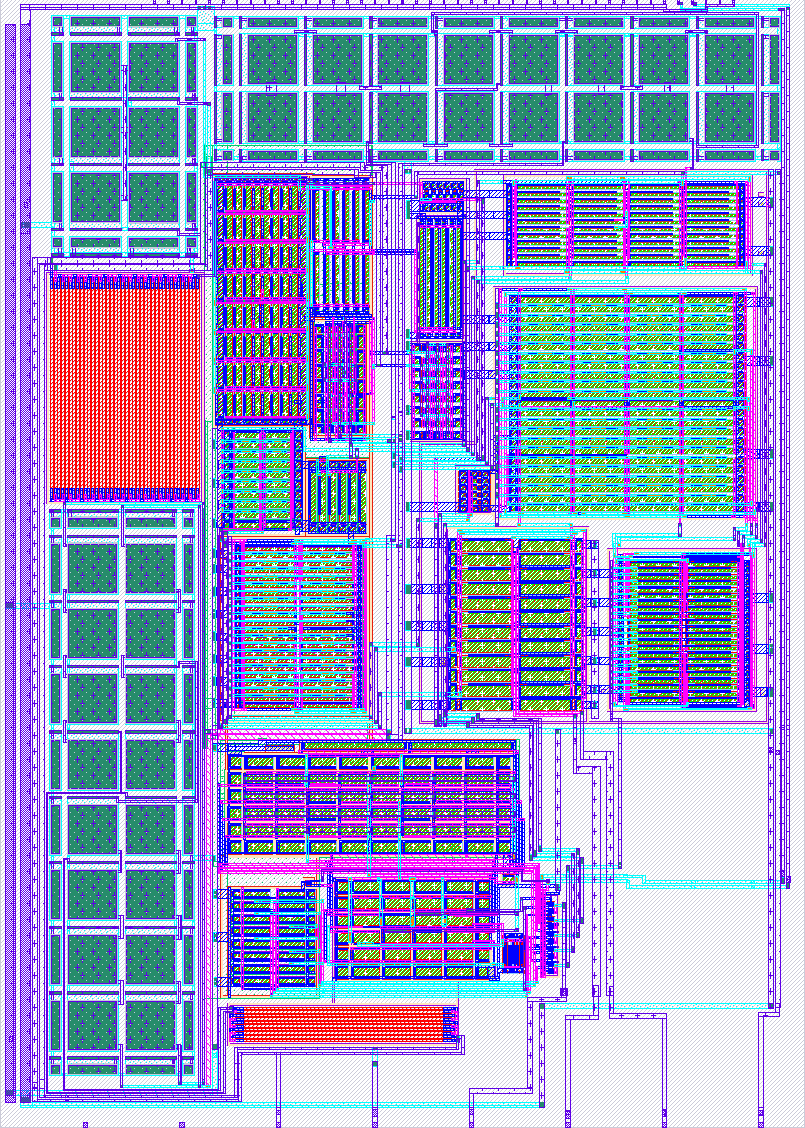
In this project, we design and tape out a fully differential two-stage operational amplifier. The architecture uses a folded cascode stage followed by a common source stage. The amplifier works as a normal fully differential op-amp.
The chip has the following connections:
- Digital inputs (2 pins): Select biasing mode (self-bias or external current source)
- Analog inputs (2 pins): Apply differential input signal
- Analog outputs (2 pins): Get the differential output signal
- Common-mode pin (1 pin): Insert the required common-mode voltage
- Power pins: Vdd (1.8 V) and Vss (ground)
How to test
We plan to use the AD03 board to test the op-amp by building a band-pass filter. During testing, we will measure:
- Standard linearity
- Offset voltage and offset current
- Common-mode rejection ratio (CMRR)
- Power supply rejection ratio (PSRR)
External hardware
The op-amp needs either:
- A resistor for self-bias, or
- An external current source, depending on the chosen biasing method.
IO
| # | Input | Output | Bidirectional |
|---|---|---|---|
| 0 | en_1 | ||
| 1 | en_2 | ||
| 2 | |||
| 3 | |||
| 4 | |||
| 5 | |||
| 6 | |||
| 7 |
Analog pins
ua | PCB Pin | Internal index | Description |
|---|---|---|---|
| 0 | A5 | 5 | Vcm |
| 1 | A0 | 0 | Vin+ |
| 2 | A4 | 4 | Vin- |
| 3 | A1 | 1 | Rgm |
| 4 | A3 | 3 | Vout+ |
| 5 | A2 | 2 | Vout- |