865 16-bit bit-serial CPU
865 : 16-bit bit-serial CPU
- Author: Tim Gu, Andrew Wang
- Description: A bit-serial CPU and 16-bit instruction architecture
- GitHub repository
- Open in 3D viewer
- Clock: 0 Hz
TinyTapeout 16-Bit-Serial CPU
Andrew Wang, Tim Gu
A bit-serial CPU processes one bit of a data word at a time using minimal logic - often reusing a small ALU and control unit across clock cycles. This is in contrast to a bit-parallel CPU, which processes entire data words (e.g., 8/16/32 bits) at once.
Processing a single bit at a time instead of in parallel means that the CPU is much slower, but it can be made much smaller. This makes the bit-serial architecture very suitable for a submission to TinyTapeout in which a chip area of 160 x 100 um is one of the primary constraints.
In this design, 16-bit width instructions are fed into the CPU over two clock cycles using the 8 TinyTapeout input signals. These instructions are decoded and the relevant operands (either immediates or stored values from a register file) are processed bit-serially from LSB to MSB and shifted into an accumulator register. The CPU supports parallel load operations to the accumulator and storing results from the accumulator to an addressable register file.
GDS Render

Functional Use (Instruction Loading)
Instruction Set
| Opcode | Mnemonic | C Operation | Description |
|---|---|---|---|
0000 |
ADDI |
acc = rs1 + imm | Add Immediate |
0001 |
SUBI |
acc = rs1 - imm | Subtract Immediate |
0010 |
SLLI |
acc = rs1 << imm | Shift left Immediate |
0011 |
SRLI |
acc = rs1 >> imm | Shift right Immediate |
0100 |
ORI |
acc = rs1 | imm | Bitwise OR Immediate |
0101 |
ANDI |
acc = rs1 & imm | Bitwise AND Immediate |
0110 |
XORI |
acc = rs1 ^ imm | Bitwise Exclusive OR Immediate |
0111 |
LOADI |
acc = imm | Load immediate into accumulator |
1000 |
ADD |
acc = rs1 + rs2 | Add Registers |
1001 |
SUB |
acc = rs1 - rs2 | Subtract Registers |
1010 |
OR |
acc = rs1 | rs2 | Bitwise OR Registers |
1011 |
AND |
acc = rs1 & rs2 | Bitwise AND Registers |
1100 |
XOR |
acc = rs1 ^ rs2 | Bitwise Exclusive OR Registers |
1101 |
LOAD |
acc = rs1 | Load from register into accumulator |
1110 |
STORE |
rs1 = acc | Store from accumulator into register |
TinyTapeout Signals Used
| Pin Group | Type | Usage |
|---|---|---|
| ui_in[7:0] | Input | Instruction bit inputs |
| uio_in[0] | Bidirectional | Pushbutton input for instruction loading |
| uo_out[7:0] | Output | Parallel output |
| clk | Clock | Clock input |
| rst_n | Reset | Active low synchronous reset |
16-bit Instruction Bit Fields
I-Type (opcode[3] == 0)
| [15:8] | [7] | [6:4] | [3:0] |
|---|---|---|---|
| immediate[7:0] | unused | rs1_addr[2:0] | opcode[3:0] |
R-Type (opcode[3] == 1)
| [15:11] | [10:7] | [6:4] | [3:0] |
|---|---|---|---|
| unused | rs2_addr | rs1_addr[2:0] | opcode[3:0] |
Instructions are loaded manually over two clock cycles via button press:
First press:
- Lower 4 bits (
ui_in[3:0]) are latched intoopcode[3:0] - Upper 4 bits (
ui_in[7:4]) go intoinstr[3:0] inst_doneis set high
Second press:
ui_in[7:0]fills ininstr[11:4]inst_doneis cleared
An edge-detected pushbutton (connected via uio_in[0]) triggers instruction loading. Once loaded, the FSM executes the instruction, and the final result is output on uo_out[7:0].
Architecture
Block Diagram
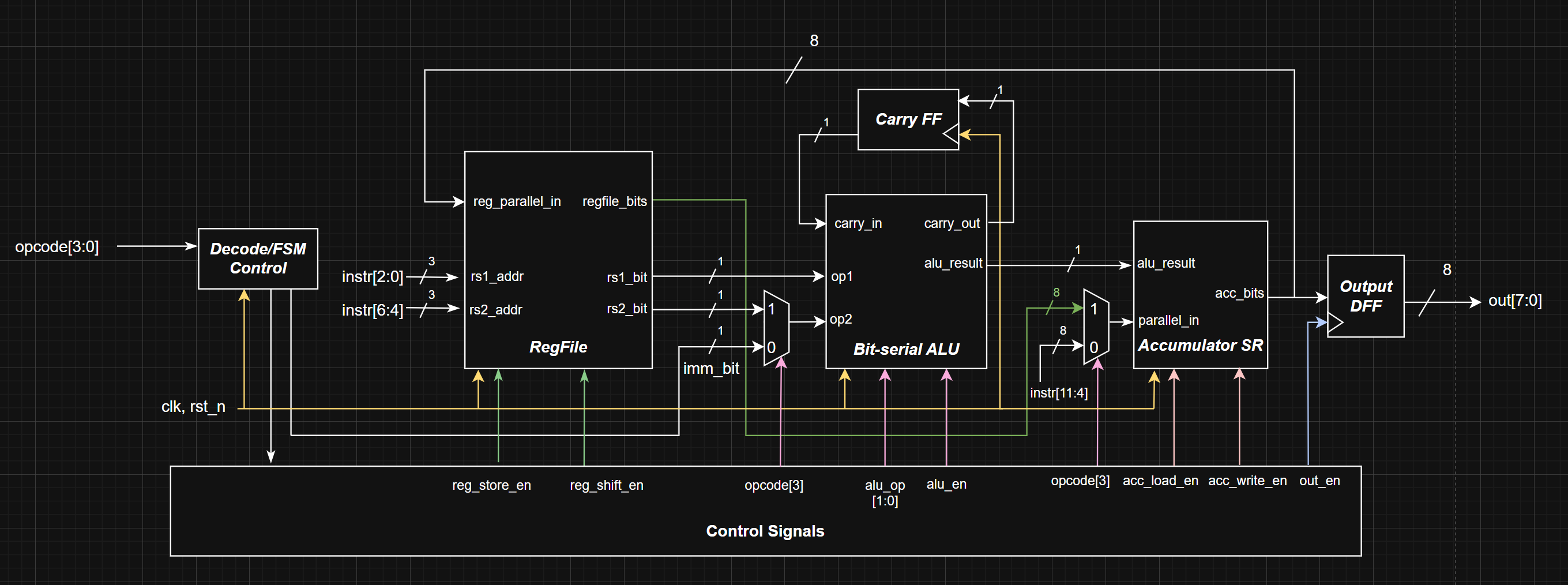
Control FSM
The fsm_control module orchestrates datapath sequencing using a 5-state FSM:
-
S_IDLE = 0x0: Waits for button press and valid instruction -
S_DECODE = 0x1: Decodes opcode, issues control signals for load/store/ALU -
S_SHIFT_REGS = 0x2: Performs serial operations; enables register shifting and accumulator writes -
S_WRITE_ACC = 0x3: Special case state for direct writes (not commonly used) -
S_OUTPUT = 0x4: Signals end of execution and enables writing to output LEDs
The FSM generates control signals including reg_shift_en, acc_write_en, alu_start, alu_op, and out_en based on instruction type.
Register File
The regfile_serial module implements an 8x8 register file, where each register is 8 bits wide. It supports:
- Serial read: each clock cycle, the bit_index increments, allowing serial bit access.
- Parallel write: a whole 8-bit register is overwritten at once from the accumulator.
- Shift operations: for shift-left/right immediate
(SLLI/SRLI), rs1_bit is offset by shift_imm, computed frominstr[6:4].
The register file outputs:
rs1_bit: used as ALU operand 1rs2_bit: used as ALU operand 2 (only valid for R-type)regfile_bits: parallel content of the selected rs1 register, forLOAD/LOADI
Bit-Serial ALU
The alu_1bit module performs a one-bit computation per cycle based on alu_op:
- Supports operations:
ADD,SUB,XOR,AND,OR, pass-through (for shift ops). carry_inandcarry_outare managed explicitly to support serial arithmetic.- For
SUB,rs2is inverted and an initial carry is injected on the first cycle.
The ALU receives rs1, rs2, alu_op, alu_start, and outputs a single-bit result to the accumulator.
Accumulator Register
The accumulator is an 8-bit shift register that:
- Loads data in parallel from
regfile_bitsorinstr[11:4](based onopcode[3]) - Receives ALU output one bit at a time via
alu_result - Tracks the write index using a delayed
bit_index_dsignal to update the correct bit and signals completion when done
The accumulator provides the final output via acc_bits.
Test Plan
This project uses a black-box testing strategy to validate the behavior of the bit-serial CPU.
- Inputs: Sequences of instructions are applied to the design via
ui_in[7:0]and a simulated pushbuttonuio_in[0]. - Outputs:
uo_out[7:0]is compared against the expected result to determine if the CPU gives the correct output. - Clock and Reset: Controlled via
clkandrst_n.
This is a clean abstraction of test logic that reflects the real-world usage model of the CPU with portability to gate-level simulations.
A cocoTB testbench is used to run tests in Python. Each test uses the following structure:
- Begin by starting the system clock and asserting/deasserting reset.
- Instructions are loaded using simulated button presses. After an instruction load, insert a delay matching the bit-serial ALU's processing time (via await ClockCycles(...)) before giving the next instruction.
- Compare
uo_outagainst the expected result usingassert_result(...). A test fails if the result mismatches or the CPU fails to update the output.
Test Coverage
full.py
- Instructions: All (R-type, I-type, LOAD, STORE, LOADI, shifts)
- Strategy: Executes a full sequence of loads, arithmetic, logical and memory ops to test integration across all instruction types.
- Modules:
- top.v
- fsm_control.v
- cpu_core.v
- regfile_serial.v
- accumulator.v
- alu_1bit.v
- Features: Full FSM flow; end-to-end bit-serial execution; regfile store/load; instruction-decode logic
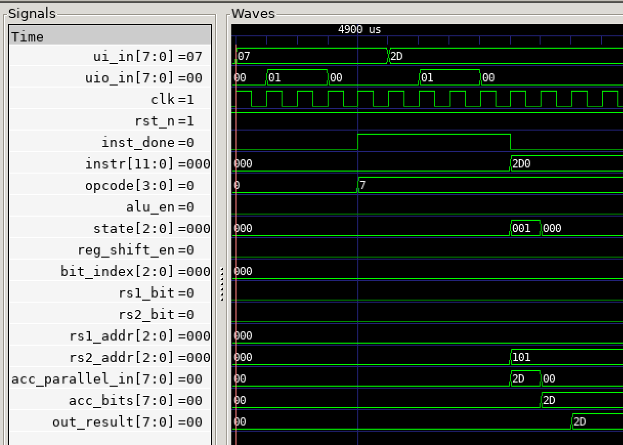
Example:
- Operation:
LOADI 0x2D - Expected result:
0x2D
alu_ops.py
- Instructions: ADD, SUB, AND, OR, XOR, LOADI, STORE
- Strategy: Loads fixed values into registers; runs R-type ALU instructions; checks accumulator result.
- Modules: fsm_control.v, cpu_core.v, regfile_serial.v, accumulator.v, alu_1bit.v
- Features: Bit-serial ALU correctness; regfile serial access; R-type decode; accumulator correctness
Example:
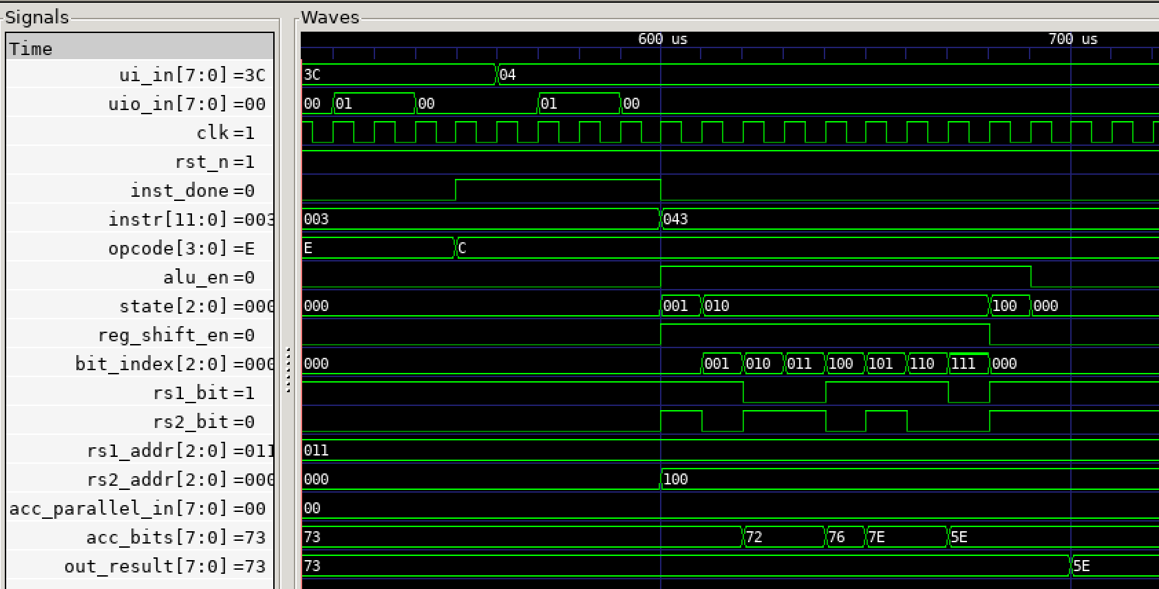
- Setup:
R3contains0x73,R4contains0x2D - Operation:
XOR R3, R4 - Expected result:
0x5E
imm_alu_ops.py
- Instructions: ADDI, SUBI, ANDI, ORI, XORI, LOADI, STORE
- Strategy: Sets known register values; executes I-type ops with immediates; checks accumulator output.
- Modules: fsm_control.v, cpu_core.v, regfile_serial.v, accumulator.v, alu_1bit.v
- Features: Immediate-decode logic; bit-serial ALU with immediate operand; regfile serial access; accumulator correctness
Example:
- Setup:
R3contains0x73,R4contains0x2D - Operation:
SUBI R3, 0x2C - Expected result:
0x47
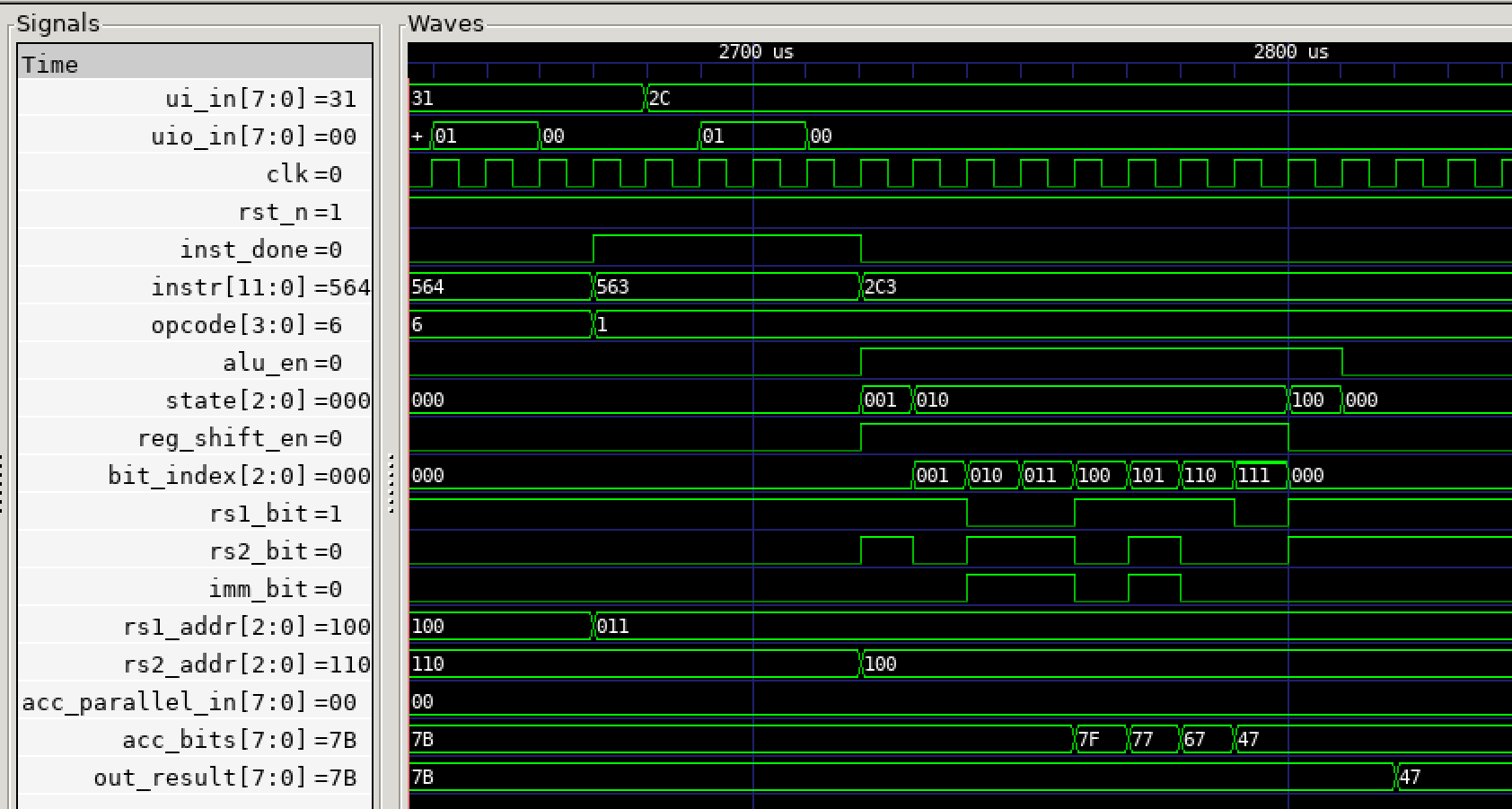
Note that in this case, the bits in the I-type instruction that correspond to the rs2 address are a value of 4. However, the mux logic correctly selects the immediate bits for use in the ALU rather than using R4 as the second operand.
shift_ops.py
- Instructions: SLLI, SRLI, LOADI, STORE
- Strategy: Loads values into registers; shifts left/right by various immediates; checks accumulator.
- Modules: fsm_control.v, cpu_core.v, regfile_serial.v, accumulator.v
- Features: Shift-index calculation; bit-serial offset-shifting; regfile serial access; accumulator correctness
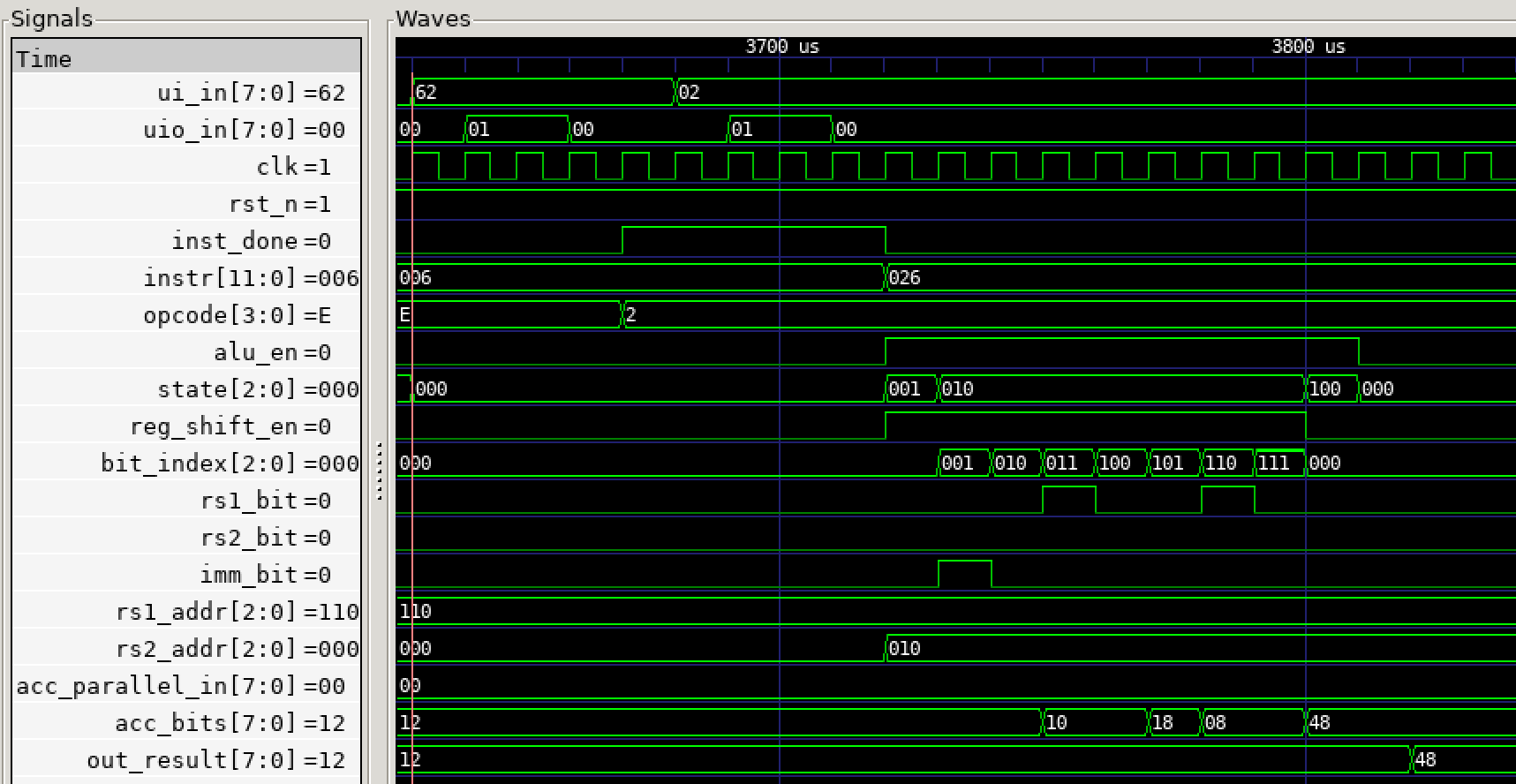
Example:
- Setup:
R6contains0x12 - Operation:
SLLI R6, 0x02 - Expected result:
0x48
Test Results
tests.full.test_alu_ops
- Status: PASS
- SIM Time: 1 650 000 ns
- Real Time: 0.02 s
- Ratio: 1.05 x 10^8 ns/s
tests.full.test_imm_alu_ops
- Status: PASS
- SIM Time: 1 660 000 ns
- Real Time: 0.02 s
- Ratio: 1.10 x 10^8 ns/s
tests.full.test_shift_ops
- Status: PASS
- SIM Time: 1 430 000 ns
- Real Time: 0.01 s
- Ratio: 1.15 x 10^8 ns/s
tests.full.test_full
- Status: PASS
- SIM Time: 3 730 000 ns
- Real Time: 0.03 s
- Ratio: 1.10 x 10^8 ns/s
- TOTAL: TESTS = 4, PASS = 4, FAIL = 0, SKIP = 0
- Aggregate SIM Time: 8 470 000 ns
- Aggregate Real Time: 0.11 s
- Overall Ratio: 7.68 x 10^7 ns/s
Project Duties & Contributions
Andrew W:
- Initial planning and design bring-up of data pipeline, instruction width, and design considerations
- Designed Verilog module hierarchy, top-level integration & module connections in
top.vandcpu_core.v - Designed and implemented the finite state machine (FSM) in
fsm_control.vfor instruction decode and control sequencing - Maintained local hardening workflow, comparing gate-level tests to GitHub CI jobs
- Debugged and fixed RTL flaws
- Documented high-level interfacing and low-level design process
Tim G:
Documentation & Planning
- Defined instruction set - opcodes, bit field layout, and supported operations for both R-type and I-type instructions
- Created the system block diagram which was used to scope out the hardware requirements for the datapath
- Wrote the test plan, identifying test cases for all instruction types and edge cases
Code Development
- Designed and implemented the bit-serial ALU and register file in
alu_1bit.vandregfile_serial.vand developed the core features required for integration of these modules. This includes R vs I-type operand multiplexing, regfile addressing, and serial arithmetic/logic operations. - Developed timing/sequencing logic for shifting the final result into the accumulator in
accumulator.v
Testbench & Simulation
- Wrote cocotb tests for each instruction category (ALU ops, shifts, immediates) and for full integration
- Debugged and verified system functionality using gtkwave simulations
IO
| # | Input | Output | Bidirectional |
|---|---|---|---|
| 0 | INST_0 | LED_0 | PB_INST |
| 1 | INST_1 | LED_1 | |
| 2 | INST_2 | LED_2 | |
| 3 | INST_3 | LED_3 | |
| 4 | INST_4 | LED_4 | |
| 5 | INST_5 | LED_5 | |
| 6 | INST_6 | LED_6 | |
| 7 | INST_7 | LED_7 |