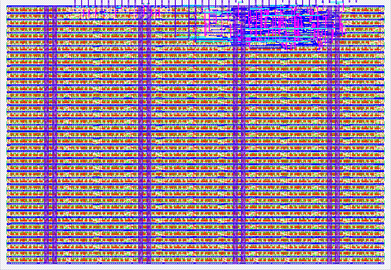
420 4-bit minicomputer ALU
420 : 4-bit minicomputer ALU

- Author: Mike McCann
- Description: this design provides basic arithmetic and logic functions
- GitHub repository
- Open in 3D viewer
- Clock: 0 Hz
How it works
The project is a 4-bit ALU section that is useful in mini and micro computer CPUs.
| Function | F2 F1 F0 | Description |
|---|---|---|
| ADD | 0 0 0 | add inputs A and B |
| AND | 0 0 1 | bitwise and operation of ports A & B |
| OR | 0 1 0 | bitwise inclusive or of ports A & B |
| XOR | 0 1 1 | bitwise exclusive or of ports A & B |
| PASSA | 1 0 0 | pass input port A unmodified |
| PASSB | 1 0 1 | pass input port B unmodified |
| SHL | 1 1 0 | shift port A left one position |
| SHR | 1 1 1 | shift port A right one position |
How to test
This device can be tested by inputting data on the two input ports (A/B), a function code (F0, F1, F2) and observing the output on pins d0, d1, d2, d3.
| Signal | Direction | Description |
|---|---|---|
| d0, d1, d2, d3 | output | function output |
| COM | input | assertion of this signal converts the output function to its 1's complement form |
| ZERO | output | this signal is asserted when the output function's value is +0 |
| NEG_ZERO | output | this signal is asserted when the output functions's value is -0 |
| ci_right | input | when performing SHL this signal shifted into position d0, when performing ADD this bit is added to output value |
| ci_left | input | when performing SHR this signal is moved into position d3, when ADDing ci_left is the input carry value |
| co_right | output | when performing SHR this signal will be equal to the unshifted value of d0 |
| co_left | output | when performing SHR this signal is equal to the unshifted value of d3, when ADDing co_left is the carry output from the addition operation |
External hardware
This project was tested using an Intel/Altera FPGA (EP2C20F484C7).
IO
| # | Input | Output | Bidirectional |
|---|---|---|---|
| 0 | da0 | d0 | NEG_ZERO |
| 1 | da1 | d1 | ci_left |
| 2 | da2 | d2 | ci_right |
| 3 | da3 | d3 | COM |
| 4 | db0 | co_left | F0 |
| 5 | db1 | co_right | F1 |
| 6 | db2 | EQU | F2 |
| 7 | db3 | ZERO |