877 8-Bit Processor with VGA
877 : 8-Bit Processor with VGA
- Author: Marcus Alagar, Derek Maeshiro, Chloe Zhong
- Description: 8-bit processor (with 16 bit instructions) that interacts with VGA
- GitHub repository
- Open in 3D viewer
- Open in VGA Playground
- Clock: 25175000 Hz
Overview
chip-w26 is a very simple 8-bit processor that also (technically) outputs to VGA. It has seven internal general-purpose 8-bit registers with one also used for VGA output and a custom ISA with eight 16-bit instructions. chip-w26 has support for up to 1024 16-bit instructions in flash memory and 256 bytes of RAM for data.
Due to constraints with using SPI for memory, chip-w26 executes a non-store/load instruction in roughly 100 clock cycles and a store/load instruction in roughly 200 clock cycles. This will almost certainly interfere with intricate VGA work, as this means between every instruction, the beam will have traced at least another 100 pixels. See more information below.
Instruction Encodings
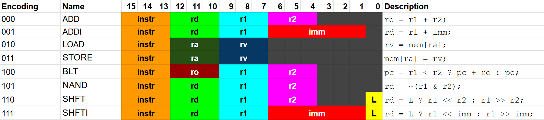
Note: For ADD, ADDI, BLT, values in input registers (r1, r2, and ro) and the immediates (imm) are treated as signed numbers using two's complement. This means that the immediate in ADDI can at most range from [-32, 31].
Note: If try to branch to a negative program counter address, is undefined behavior. i.e. BLT (-6) (0) (1) as the 0th instruction (where program counter would be 0).
Note: Technically can branch to an unaligned address. Highly discouraged.
Memory
chip-w26, for simplicity, uses the flash memory exclusively for instructions and RAM exclusively for data. Therefore, the address stored in the program counter, which increments by 2 after each instruction, is different from the addresses that the processors LOADs from and STOREs into.
The program counter is 11 bits wide, allowing access to up to 2048 bytes. However, since every instruction is 16 bits, each instruction takes up two bytes. Thus, after normally executing an instruction (and not branching), the program counter automatically increments by 2.
Instructions are assumed to be stored in a big-endian style.
                 5432109876543210
1st instruction: abcdefghijklmnop
2nd instruction: qrstuvwxyzabcdef
memory:
addr | data
-----------
 0   | abcdefgh
 1   | ijklmnop
 2   | qrstuvwx
 3   | yzabcdef
The first instruction fetched will always be at address 0 in flash memory.
RAM accesses, through LOAD and STORE can address up to a value stored in one of the registers. In other words, only addresses representable in 8 bits are available. This means there are 256 bytes of read/write RAM available.
Register Mappings
reg | desc
----------
r0  | R , always zero
r1  | RW, general-purpose
r2  | RW, general-purpose
r3  | RW, general-purpose
r4  | RW, general-purpose
r5  | RW, general-purpose
r6  | RW, general-purpose
r7  | RW, r7[5:0] is attached to {r[1:0], g[1:0], b[1:0]},
    |     with an automatic check to see if is in
    |     display range to not hurt the VGA screen
How to test
Pull rst_n low, then flash desired program within the first 2048 bytes. Once let rst_n go high and start clocking, processor will begin fetching from address 0 and program (should) start running!
Note that programs should end with an infinite loop or expect to restart once the program counter overflows.
External hardware
Referring to the 3 PMOD headers on the default TT demo board:
INPUT: None.
BIDIR: QSPI PMOD for flash and RAM.
OUTPUT: TinyVGA PMOD to drive a VGA screen.
IO
| # | Input | Output | Bidirectional |
|---|---|---|---|
| 0 | R[1] | CS0 (Flash) | |
| 1 | G[1] | MOSI | |
| 2 | B[1] | MISO | |
| 3 | VSYNC | SCK | |
| 4 | R[0] | NC | |
| 5 | G[0] | NC | |
| 6 | B[0] | CS1 (RAM A) | |
| 7 | HSYNC | CS2 (RAM B) |