112 Genesis
112 : Genesis
- Author: brunny95
- Description: 8-phase buck converter + ultra low power BG
- GitHub repository
- Open in 3D viewer
- Clock: 0 Hz
How it works
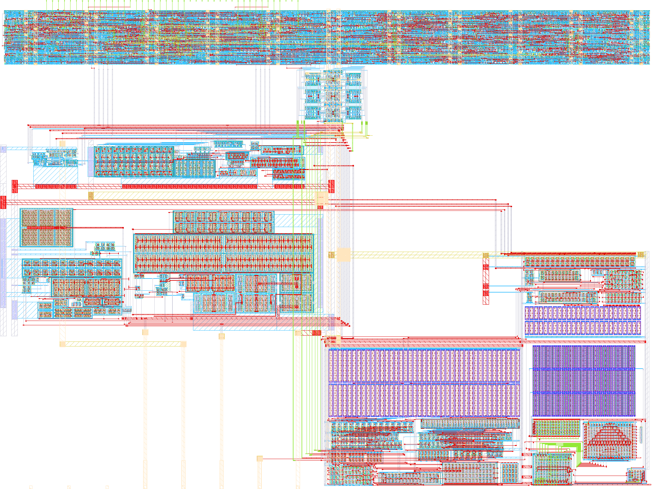
This design is a mixed-signal 8-phase buck converter controller. The digital block (top_dig) manages startup sequencing, soft-start, phase rotation, and digital configuration, while the analog blocks generate the control-oriented signals used by the digital logic and implement the regulation loop.
At top level, the system is composed of:
- a bias/reference generation path,
- level shifters between digital low-voltage control and analog control domains,
- an analog control block (
ctrl), - the digital sequencing block (
top_dig/top_dig2).
Although cot and hs_req are inputs of the top_dig module, they are not external system inputs at top level. They are generated internally by the analog control path:
cotis produced by the analog control block and indicates when a new switching event is needed,hs_reqis generated by the analog control path and is used by the digital block to terminate soft-start and enter normal operation.
Digital control flow
The digital controller is organized around a 4-state FSM:
- IDLE: waiting for controller enable.
- DEADTIME: after enable, the controller forces the comparator high for a fixed 1.6 ms startup delay.
- SOFTSTART: switching activity is introduced gradually through a DDS-based ramp.
- RUN: normal operation.
If soft-start bypass is enabled, the controller skips the DEADTIME and SOFTSTART phases and goes directly to RUN.
Soft-start operation
During soft-start, the digital block does not forward switching activity directly from the analog request path. Instead, pulse generation is modulated by an internal DDS ramp:
- a programmable initial increment sets the startup pulse rate,
- the DDS increment increases over time,
- the pulse density progressively ramps up until
hs_reqindicates the end of soft-start.
This provides controlled startup of the converter and avoids abrupt energy delivery.
Phase management
The controller supports from 1 to 8 active phases, configured through cfg_n_ph.
A phase counter rotates across the enabled phases and generates a one-hot phase selection for the high-side outputs. This distributes switching events across the active phases in round-robin fashion.
Output generation
The high-side outputs are exposed on uio_out[7:0], with corresponding enables on uio_oe[7:0].
Depending on configuration:
- in forced CCM mode, the controller emits one-hot phase pulses,
- otherwise, enabled phases remain statically asserted according to the selected operating mode.
Unused phases can optionally be driven low through cfg_unused_force_low.
Configuration interface
The digital block contains a 38-bit serial configuration shift register. Configuration is loaded through:
SR_DATA,SR_CLK,SR_COMMIT.
The register controls:
- soft-start bypass,
- external reference forcing,
- soft-start startup frequency,
- TON selection,
- number of active phases,
- reference trim and reference source selection,
- external capacitor enable,
- high-gm mode,
- forced CCM,
- debug mux routing.
Analog / digital interaction
The analog block ctrl implements the regulation path and generates the internal control signals observed by the digital sequencer. In particular:
- the analog comparator and delay path generate
cot, - the analog startup/control path generates
hs_req, - the digital block returns control signals such as
force_comp_high,ss_done,en_ctrl2_1p2v, andsel_ton_1p2vback to the analog domain.
This makes the overall architecture a closed mixed-signal control loop rather than a purely digital pulse generator.
Debug outputs
Several internal digital signals can be routed to the dedicated outputs through a debug mux, including:
cot,hs_req,- FSM state bits,
force_comp_high,ss_active,ss_done,hs_pulse,- DDS
tick, - control enable signals.
This is useful for bring-up, mixed-signal validation, and lab/debug correlation.
How to test
The design should be tested as a mixed-signal controller, verifying both the digital sequencing and the interaction with the internally generated analog control signals.
Basic startup test
- Reset the design and keep
en_ctrl_1p2vlow. - Release reset and enable the controller.
- Verify the FSM transitions:
IDLE -> DEADTIME -> SOFTSTART -> RUN
- Check that:
force_comp_highis asserted only during DEADTIME,ss_activeis asserted only during SOFTSTART,ss_doneis asserted only during RUN.
Soft-start bypass test
- Enable soft-start bypass through
ss_bypass_extorcfg_ss_bypass. - Enable the controller.
- Verify that the state machine enters RUN directly.
Analog interface test
- Verify that
cotis generated by the analogctrlblock and observed correctly by the digital controller. - Verify that
hs_reqis generated internally by the analog control path. - Check that deasserting
hs_reqcauses the transition from SOFTSTART to RUN.
DDS soft-start test
- Run with soft-start enabled.
- Observe
tick,hs_pulse,ss_active, andhs_req. - Verify that:
- DDS is initialized at SOFTSTART entry,
- the pulse activity starts from the programmed initial rate,
- the pulse density increases over time,
- soft-start terminates only when
hs_reqends soft-start.
Phase rotation test
- Program
cfg_n_phfrom 0 to 7. - Verify that the number of enabled phases is respectively 1 to 8.
- In RUN mode, verify that switching requests are distributed round-robin across active phases only.
CCM mode test
- Test with
cfg_fccm = 0andcfg_fccm = 1. - Verify that
FORCE_CCMis asserted only in RUN when enabled by configuration. - Check output behavior in both normal and forced-CCM operation.
Configuration register test
- Shift known values into the serial configuration register.
- Commit the configuration.
- Verify correct update of:
- TON selection,
- number of phases,
- reference settings,
- external capacitor enable,
- high-gm mode,
- force-CCM mode,
- debug mux selections.
Debug test
- Route internal signals to the debug outputs.
- Verify visibility of relevant signals such as
cot,hs_req,ss_active,ss_done,tick, andhs_pulse.
Disable / reset test
- Disable the controller from each FSM state.
- Verify return to IDLE and reset of internal counters and startup state.
IO
| # | Input | Output | Bidirectional |
|---|---|---|---|
| 0 | EN_BIAS_1P2V | FORCE_CCM | HS_OUT[0] |
| 1 | EN_CTRL_1P2V | DISB_N | HS_OUT[1] |
| 2 | VC_PULL_DOWN | SS_ACTIVE | HS_OUT[2] |
| 3 | SS_BYPASS_EXT | SR_OUT | HS_OUT[3] |
| 4 | THWN | DBG_4 | HS_OUT[4] |
| 5 | SR_COMMIT | DBG_5 | HS_OUT[5] |
| 6 | SR_DATA | DBG_6 | HS_OUT[6] |
| 7 | SR_CLK | DBG_7 | HS_OUT[7] |
Analog pins
ua | PCB Pin | Internal index | Description |
|---|---|---|---|
| 0 | A0 | 0 | VDDA |
| 1 | A1 | 1 | EXT_REF |
| 2 | A2 | 2 | FB_VOUT |
| 3 | A3 | 3 | FB_SW |
| 4 | A4 | 4 | VC |