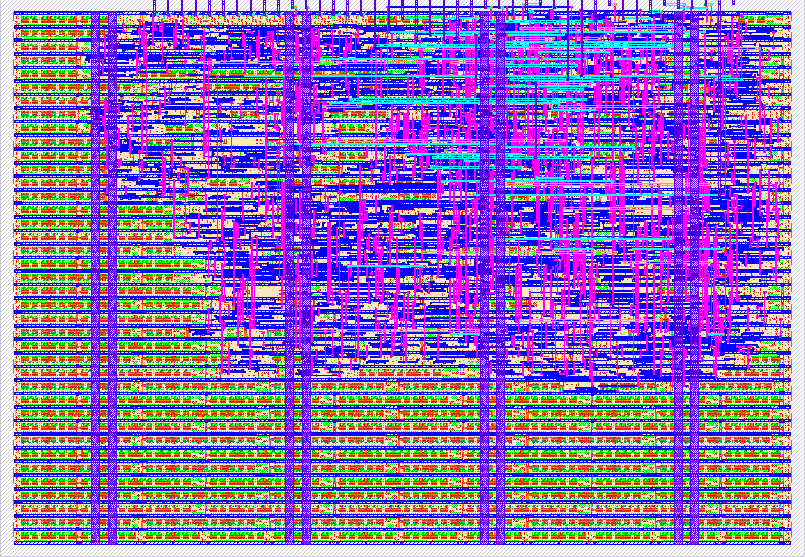
419 Sky130 Digital Playground
419 : Sky130 Digital Playground

- Author: Eduardo Holguin
- Description: Select and test eight classic digital blocks (gates, 8-bit counter, PWM, 7-seg, 4-bit ALU, FDC, 16×4 RAM, and turn signals) on a single TinyTapeout Sky130 tile.
- GitHub repository
- Open in 3D viewer
- Clock: 0 Hz
How it works
Mode is selected with ui_in[2:0] (exclusive; only these three bits choose the active block).
All other pins either feed the active block or are ignored by the top.
The top builds a full 8-bit uo_out value for each mode and forces all unused bits to 0.
Bidirectional pads are inputs only in this design: uio_out = 0x00 and uio_oe = 0x00, so there is no contention on uio[*].
clk drives the Counter, PWM, RAM, FDC registers, and the turn-signal timing. rst_n is active-low (internally inverted for FDC which expects active-high).
Pin summary:
- Dedicated inputs:
ui_in[7:0]ui_in[2:0]= mode (exclusive)- Other
ui_inbits are used as control/address in some modes (see mode map).
- Bidirectional (used as inputs only):
uio_in[7:0] - Dedicated outputs:
uo_out[7:0](all bits defined per mode; unused bits = 0)
Mode map (ui_in[2:0])
000 Basic gates
Inputs: uio_in[0]=a, uio_in[1]=b
Outputs: uo_out = {00, ~a, NOR, NAND, XOR, OR, AND}
001 8-bit Counter
Inputs: ui_in[3]=EN (1 = count), uses global clk and rst_n
Outputs: uo_out = count[7:0] (increments on each clk edge while EN=1; clears on !rst_n)
010 PWM (8-bit)
Inputs: uio_in[7:0]=duty
Outputs: uo_out = {duty[7:1], pwm}
011 HEX to 7-segment
Inputs: uio_in[3:0]=hex
Outputs: uo_out = {0, seg[6:0]} where seg={a,b,c,d,e,f,g}, 1=ON
100 Mini-ALU (4-bit)
Inputs: uio_in[3:0]=A, uio_in[7:4]=B, ui_in[5:3]=op
op: 000 add, 001 sub, 010 AND, 011 OR, 100 XOR, 101 NOTA, 110 PASSA, 111 PASSB
Outputs: uo_out = {000, flag, Y[3:0]} (flag = carry or !borrow)
101 FDC (frequency discriminator)
Inputs: uio_in[0]=VCO (external square wave); uses global clk and rst_n
Outputs: uo_out = {000, D_out[4:0]}
110 RAM 16x4 (synchronous read, 2-cycle pipelined WE)
Inputs: ui_in[7]=WE, ui_in[6:3]=ADDR, uio_in[3:0]=DATA_IN
Outputs: uo_out = {0000, DATA_OUT[3:0]}
111 Direccionales (turn signals)
Inputs: ui_in[4:3]=dir (01 left, 10 right, 11 both)
Outputs: uo_out = {0, right[2:0], 0, left[2:0]}
How to test
General: set mode with ui_in[2:0], then drive the listed inputs and read uo_out[7:0].
GATES (000): drive a,b on uio_in[1:0]; check uo_out matches {00, ~a, NOR, NAND, XOR, OR, AND}.
COUNTER (001): set ui_in[3]=1 to enable; observe uo_out[7:0] increment each clk. Assert rst_n=0 to clear to 0. Set ui_in[3]=0 to hold the count.
PWM (010): write duty to uio_in[7:0]; measure uo_out[0] with a scope; duty cycle ≈ duty/256; uo_out[7:1] shows duty[7:1].
HEX7 (011): write hex nibble to uio_in[3:0]; uo_out[6:0] emits segment bits (active-high). Invert externally if your display is common-anode.
ALU (100): set A=uio_in[3:0], B=uio_in[7:4], op=ui_in[5:3]; read Y on uo_out[3:0] and carry/!borrow on uo_out[4].
FDC (101): feed a square wave into uio_in[0]; uo_out[4:0] changes with frequency; rst_n resets state.
RAM (110): write by setting ADDR=ui_in[6:3], DATA_IN=uio_in[3:0], WE=ui_in[7]=1 for a few clocks (internal WE pipeline); read with WE=0 and same ADDR; after one clock uo_out[3:0] shows DATA_OUT.
Direccionales (111): dir=ui_in[4:3]; left pattern on uo_out[2:0]; right pattern on uo_out[6:4] (secuencia 001→011→111).
Safety notes
uio_outanduio_oeare always 0;uio_incan be tied to switches or sources without bus contention.- Use series resistors for LEDs (330 to 1000 Ω).
- Keep input levels within IO voltage (e.g., 3.3 V).
External hardware
- 8 LEDs + 8 resistors (to view
uo_out[7:0]) - DIP switches / jumpers / PMOD-Switch (to drive
uio_in[7:0]) - Single 7-segment display + resistors (HEX7 mode)
- Function generator (0 to VDD square) for FDC input on
uio_in[0] - Logic analyzer or oscilloscope (PWM duty, RAM timing, FDC response)
IO
| # | Input | Output | Bidirectional |
|---|---|---|---|
| 0 | MODE_SEL0 | OUT0 (mode-dep: GATES_AND | CNT_Q0 | PWM_OUT | HEX7_SEG_G | ALU_Y0 | FDC_D0 | RAM_Q0 | DIR_IZQ0) | GEN0: GATES_A / FDC_VCO / PWM_DUTY0 / HEX_X0 / ALU_A0 |
| 1 | MODE_SEL1 | OUT1 (mode-dep: GATES_OR | CNT_Q1 | PWM_DUTY1 | HEX7_SEG_F | ALU_Y1 | FDC_D1 | RAM_Q1 | DIR_IZQ1) | GEN1: GATES_B / PWM_DUTY1 / HEX_X1 / ALU_A1 |
| 2 | MODE_SEL2 | OUT2 (mode-dep: GATES_XOR | CNT_Q2 | PWM_DUTY2 | HEX7_SEG_E | ALU_Y2 | FDC_D2 | RAM_Q2 | DIR_IZQ2) | GEN2: PWM_DUTY2 / HEX_X2 / ALU_A2 |
| 3 | AUX0 / CNT_EN / RAM_A0 / ALU_OP0 / DIR0 | OUT3 (mode-dep: GATES_NAND| CNT_Q3 | PWM_DUTY3 | HEX7_SEG_D | ALU_Y3 | FDC_D3) | GEN3: PWM_DUTY3 / HEX_X3 / ALU_A3 |
| 4 | AUX1 / RAM_A1 / ALU_OP1 / DIR1 | OUT4 (mode-dep: GATES_NOR | CNT_Q4 | PWM_DUTY4 | HEX7_SEG_C | ALU_FLAG | FDC_D4 | DIR_DER0) | GEN4: PWM_DUTY4 / ALU_B0 |
| 5 | AUX2 / RAM_A2 / ALU_OP2 | OUT5 (mode-dep: GATES_NOT_A | CNT_Q5 | PWM_DUTY5 | HEX7_SEG_B | DIR_DER1) | GEN5: PWM_DUTY5 / ALU_B1 |
| 6 | AUX3 / RAM_A3 | OUT6 (mode-dep: CNT_Q6 | PWM_DUTY6 | HEX7_SEG_A | DIR_DER2) | GEN6: PWM_DUTY6 / ALU_B2 |
| 7 | RAM_WE | OUT7 (mode-dep: CNT_Q7 | PWM_DUTY7) | GEN7: PWM_DUTY7 / ALU_B3 |