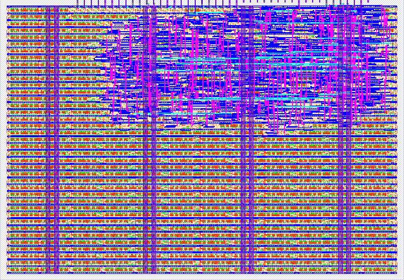
37 Design of SRAM BIST
37 : Design of SRAM BIST

- Author: Surabhi A S, Gokul Krishnan V, G R Deepakkumar, Bhoomika K M, Vedashree B S, Shylashree N, RV College of Engineering, Bengaluru
- Description: Design of SRAM BIST
- GitHub repository
- Open in 3D viewer
- Clock: 0 Hz
Credits
We gratefully acknowledge the Center of Excellence (CoE) in Integrated Circuits and Systems (ICAS) and the Department of Electronics and Communication Engineering (ECE) for providing the necessary resources and guidance.
Special thanks to Dr. H V Ravish Aradhya (HoD- ECE), Dr. K R Usha Rani (Associate Dean-PG), Dr. K. S. Geetha (Vice Principal) and Dr. K. N. Subramanya (Principal) for their constant encouragement and support in facilitating this Tiny Tapeout SKY25A submission.
How it works
The tt_um_mbist module implements a basic Built-In Self-Test (BIST) mechanism for an 8-bit × 16-word internal SRAM. It uses a simple Finite State Machine (FSM) to write and read test patterns from the SRAM to verify memory integrity.
The input control bus ui_in is structured as:
- [7] → start: Initiates the BIST process.
- [6] → write_en: Optional write enable for extending usage.
- [5:4] → mode: Reserved for future modes of test (e.g., walking 1s/0s).
- [3:0] → data_in: 4-bit test pattern (padded to 8 bits).
During the test:
- On start, the FSM writes the data_in pattern to all SRAM addresses (padded with 0000 in MSBs).
- Then it reads back each location and compares it with the expected value.
- If any mismatch is found, a fail flag is set.
- Upon completion, a done flag is raised.
Outputs are delivered via uo_out:
- [7] → done: Test complete indicator.
- [6] → fail: Test failed flag.
- [5:0] → Reserved/debug.
Functional Description
Input and Output Ports
-
Inputs:
- clk – System clock (e.g., 10 µs period or 100 kHz)
- rst_n – Active-low asynchronous reset
- ena – Always high (used internally to suppress unused signal warnings)
- ui_in[7:0] – Control input bus:
- [7] Start BIST
- [6] Write Enable (optional/future use)
- [5:4] Mode Select
- [3:0] Data Input (test pattern)
- uio_in[7:0] – Optional address input (only uio_in[3:0] used)
-
Outputs:
- uo_out[7:0] – BIST status output:
- [7] Done
- [6] Fail
- [5:0] Reserved/debug
- uio_out[7:0] – Unused, driven low
- uio_oe[7:0] – Output enable, all set to input (driven low)
- uo_out[7:0] – BIST status output:
Internal Architecture
FSM Operation
The module uses a simple 2-bit FSM with the following states:
- IDLE – Wait for start signal
- WRITE – Write data_in to all addresses
- READ – Read and compare each address against expected pattern
- DONE – Output done and fail flags
SRAM Array
The design includes an internal 16×8-bit SRAM array (mem[0:15]). Writes and reads are synchronized with the clock.
Output Encoding
- When the BIST finishes, uo_out[7] is set high.
- If any data mismatch is detected during read-back, uo_out[6] is also set high.
Reset Behavior
- rst_n clears the FSM to IDLE.
- Clears fail and done flags.
- Resets address pointer.
How to Test
A Cocotb-based Python testbench is recommended. The typical procedure is:
- Assert rst_n low → then high to initialize.
- Drive a value on ui_in[3:0] (e.g., 4'hA).
- Assert ui_in[7] to start the test.
- Wait until uo_out[7] (done) is high.
- Check uo_out[6] to determine pass/fail.
Example Test Scenarios
| Test Pattern | ui_in[3:0] | Behavior | Expected uo_out |
|---|---|---|---|
| 0xA | 4'b1010 | All memory set to 0x0A | Done=1, Fail=0 |
| 0xF | 4'b1111 | All memory set to 0x0F | Done=1, Fail=0 |
| Altered mem | N/A | Inject mismatch before READ | Done=1, Fail=1 |
Simulation Monitoring
To monitor values in simulation (Verilog), include:
initial begin
    $monitor("Time=%0t | Start=%b Addr=%d DataIn=0x%0h ReadBack=0x%0h | Done=%b Fail=%b",
              $time, ui_in[7], addr, ui_in[3:0], mem[addr], uo_out[7], uo_out[6]);
end
IO
| # | Input | Output | Bidirectional |
|---|---|---|---|
| 0 | DATA_IN[0] | ||
| 1 | DATA_IN[1] | ||
| 2 | DATA_IN[2] | ||
| 3 | DATA_IN[3] | ||
| 4 | MODE[0] | ||
| 5 | MODE[1] | ||
| 6 | WRITE_EN | FAIL | |
| 7 | START | DONE |