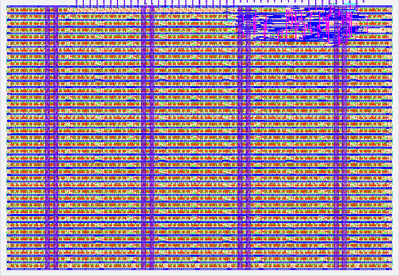
41 Pulse Width Encoder
41 : Pulse Width Encoder

- Author: Chandan N,Gurudatt B M,Akshay Pattar,Amogh Y N,Revanna J T, Shylashree N, RV College of Engineering, Bengaluru
- Description: Design of Pulse Width Encoder
- GitHub repository
- Open in 3D viewer
- Clock: 100 Hz
Credits
We gratefully acknowledge the Center of Excellence (CoE) in Integrated Circuits and Systems (ICAS) and the Department of Electronics and Communication Engineering (ECE) for providing the necessary resources and guidance. Special thanks to Dr. K R Usha Rani (Associate Dean - PG), Dr. H V Ravish Aradhya (HOD-ECE), Dr. K. S. Geetha (Vice Principal) and Dr. K. N. Subramanya (Principal) for their constant encouragement and support to carry out this Tiny Tapeout SKY25A submission.
How it works
The tt_um_pwe module is a Pulse Width Encoder (PWE) designed to generate a digital pulse of programmable width based on user-controlled input signals. This module receives a 4-bit width value along with control signals (start and enable) and responds by generating a pulse_out signal that remains high for the specified number of clock cycles. Upon completion, it raises a done flag for one clock cycle to indicate the end of the pulse generation sequence.
At the heart of the module is a Finite State Machine (FSM) that coordinates the pulse generation sequence across three well-defined states: IDLE, COUNTING, and DONE. This enables the design to operate predictably and synchronously, even when integrated into larger digital systems. The design is clock-driven and fully synchronous, with a global asynchronous active-low reset (rst_n) to initialize the internal states.
Functional Description
Input and Output Ports
Inputs
-
ui_in(8 bits):ui_in[0]- start: Initiates the pulse generation cycle when high.ui_in[1]- enable: Must be high in conjunction withstartto trigger the pulse.ui_in[5:2]- data_in: 4-bit value specifying the pulse width (in clock cycles).ui_in[6],ui_in[7]- Unused; internally tied off to suppress lint warnings.
-
uio_in(8 bits): General-purpose I/O input (not used in this design). -
clk- Clock signal for all sequential logic. -
rst_n- Active-low asynchronous reset.
Outputs
-
uo_out(8 bits):uo_out[0]- pulse_out: High during the pulse generation phase.uo_out[1]- done: High for one cycle after the pulse completes.uo_out[7:2]- Unused; set to zero.
-
uio_out,uio_oe(8 bits each): Not used; tied to zero to act as high-impedance inputs.
Internal Architecture
Finite State Machine (FSM)
The FSM governs the behavior of the module with the following states:
-
IDLE:
- Waits for
startandenablesignals. - When both are high, captures the value of
data_inand stores it in the internalcounter. - Transitions to the
COUNTINGstate.
- Waits for
-
COUNTING:
- Asserts
pulse_outhigh. - Decrements
counteron each clock cycle. - When
counterreaches zero, transitions to theDONEstate.
- Asserts
-
DONE:
- Deasserts
pulse_outand setsdonehigh for a single clock cycle. - Transitions back to
IDLE.
- Deasserts
This sequencing ensures precise pulse generation, avoids glitches, and guarantees a clean done signal after pulse completion.
Pulse Width Logic
- The value in
data_indetermines the number of clock cycles thepulse_outremains high. - The
counterregister is initialized withdata_inand decremented every cycle in theCOUNTINGstate. - Pulse generation is fully synchronous with the
clksignal.
Reset Behavior
- When
rst_nis low:- The FSM resets to
IDLE. - Registers like
counter,pulse_width,pulse_out, anddoneare cleared to zero. - Ensures safe and deterministic startup.
- The FSM resets to
Unused Logic Handling
- All unused inputs (
uio_in,ui_in[6],ui_in[7]) are logically consumed using a bitwise AND expression to suppress unused signal warnings. - All unused outputs (
uio_out,uio_oe) are set to zero.
How to Test
To validate the tt_um_pwe design, a testbench (tt_um_pwe_tb.v) is used to simulate various scenarios where different pulse widths are provided. The testbench monitors the outputs pulse_out and done and checks their timing against the expected behavior.
Example Test Scenarios
| Time (ns) | ui_in[5:2] (Pulse Width) | start | enable | Expected Behavior |
|---|---|---|---|---|
| 0 – 10 | 0000 (0) | 0 | 0 | No operation |
| 10 – 30 | 0100 (4) | 1 | 1 | 4-cycle pulse, then done |
| 30 – 60 | 0011 (3) | 1 | 1 | 3-cycle pulse, then done |
| 60 – 90 | 0001 (1) | 1 | 1 | 1-cycle pulse, then done |
| 90 – 100 | 0000 | 0 | 0 | Remains in IDLE |
During each simulation cycle:
pulse_outshould remain high fordata_innumber of clock cycles.doneshould pulse high for exactly one cycle afterpulse_outdeasserts.
Monitoring Output
During simulation, real-time debugging and waveform inspection help verify that the FSM and counter logic work as intended.
Use the following $monitor statement in the testbench:
initial begin
  $monitor("Time=%0t | start=%b enable=%b data_in=%b | pulse_out=%b done=%b", $time, ui_in[0], ui_in[1], ui_in[5:2], pulse_out, done);
end
IO
| # | Input | Output | Bidirectional |
|---|---|---|---|
| 0 | ui_in[0] | uo_out[0] | |
| 1 | ui_in[1] | uo_out[1] | |
| 2 | ui_in[2] | ||
| 3 | ui_in[3] | ||
| 4 | ui_in[4] | ||
| 5 | ui_in[5] | ||
| 6 | |||
| 7 |