868 Analog design
868 : Analog design
- Author: Zedulo
- Description: A tri 2 -input AND gate (7408 compatible) and an SR Latch
- GitHub repository
- Open in 3D viewer
- Clock: 0 Hz
How it works
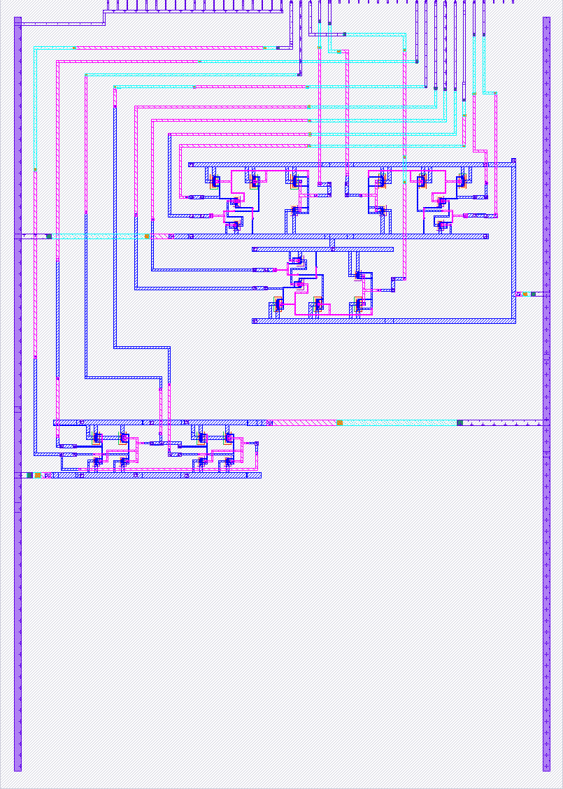
For SR LATCH This project implements an SR latch using two cross-coupled NOR gates. The output of each NOR gate is fed back into one input of the other, forming a bistable circuit.
When s(set) is asserted high, the latch sets q=1 and qb=0. Wheh r(reset) is asserted high, the latch resets q=0 and qb=1. When both inputs are low, the latch holds its previous state due to the feedback structure.
The condition s=1 and r=1 is invalid because it forces both outputs low and can lead to an undefined state when released.
For AND IC gate 7408 The project is a custom silicon implementation of the classic 7408 Tri 2-input AND gate. Unlike standard digital projects that use pre-designed logic libraries, this design was built from the transistor level using a CMOS analog design flow.
Logic Implementation: It consists of three independent 2-input AND gates. Transistor Level: Each gate uses a custom NMOS and PMOS transistor topology to perform the logical AND function. Power Domain: The design operates on the VDPWR (1.8V) digital power rail and utilizes VGND as the common ground reference. Signal Path: Inputs are received through the dedicated input pads, processed by the CMOS logic, and driven out through the dedicated output pads. ESD Protection: The design relies on the pre-installed ESD (Electrostatic Discharge) protection provided by the Tiny Tapeout padring, removing the need for internal protection diodes that could interfere with spice generation.
How to test
For SR LATCH
- Apply power 1.8V to vdd of the circuit, and gnd to gnd terminal of the source.
- Set both s and r to 0 --> the latch should hold its previous state.
- set s=1 and r=0 --> q should go high
- Return s to 0 --> q should remain high, i.e state is stored
- Set r=1 and s=0 --> q should go low
- Return r to 0 --> q should remain low
You can verify using these operations:
- Simulation (transient analysis in xschem/ngspice)
- Observing q and qb on output pins in hardware
For AND gate IC 7408 To verify the functionality of the 7408 AND IC, you must provide logic signals to the input pairs and monitor the output state.
-
Ensure the chip is powered with 1.8V on the VDPWR pin.
-
Apply 1.8V (Logic 1) or 0V (Logic 0) to an input pair.
-
Monitor the corresponding output.
-
Truth Table Validation: The output Y1 should only go High (1.8V) if both A1 AND B1 are High. In all other combinations (00, 01, 10, 11), the output must remain Low (0V).
-
Perform the same check for Gates 2 and 3 using their respective pin mappings defined in the info.yaml
Pin Connection
For SR Latch
- s (ui_in[7])
- r (ui_in[6])
- qb (uo_out[4])
- q (uo_out[3])
For AND gate IC 7408
- A1 (ui_in[2])
- B1 (ui_in[3])
- Y1 (uo_out[1])
- A2 (ui_in[1])
- B2 (ui_in[0])
- Y2 (uo_out[0])
- A3 (ui_in[5])
- B3 (ui_in[4])
- Y3 (uo_out[2])
External hardware
For AND gate IC 7408 To interact with this project in a physical lab setting, the following external hardware is required:
-
Logic Inputs: 6x Push buttons or DIP switches to provide logic states to the input pins.
-
Logic Indicators: 3x LEDs (with current-limiting resistors, typically 330Ω) connected to the output pins to visualize the AND gate outputs.
-
Breadboard/PMOD: A standard PMOD connector or breadboard interface to bridge the Tiny Tapeout carrier board to your external components.
-
Power Supply: A stable 1.8V DC source if not using the regulated output from the Tiny Tapeout demonstration board.
For SR Latch No external hardware is required!
The design operates as a standalone digital logic block and can be tested using simulation tools or integrated into a larger digital system
IO
| # | Input | Output | Bidirectional |
|---|---|---|---|
| 0 | B2 | Y2 | |
| 1 | A2 | Y1 | |
| 2 | A1 | Y3 | |
| 3 | B1 | q | |
| 4 | B3 | qb | |
| 5 | A3 | ||
| 6 | r | ||
| 7 | s |