166 AstraPIO
166 : AstraPIO
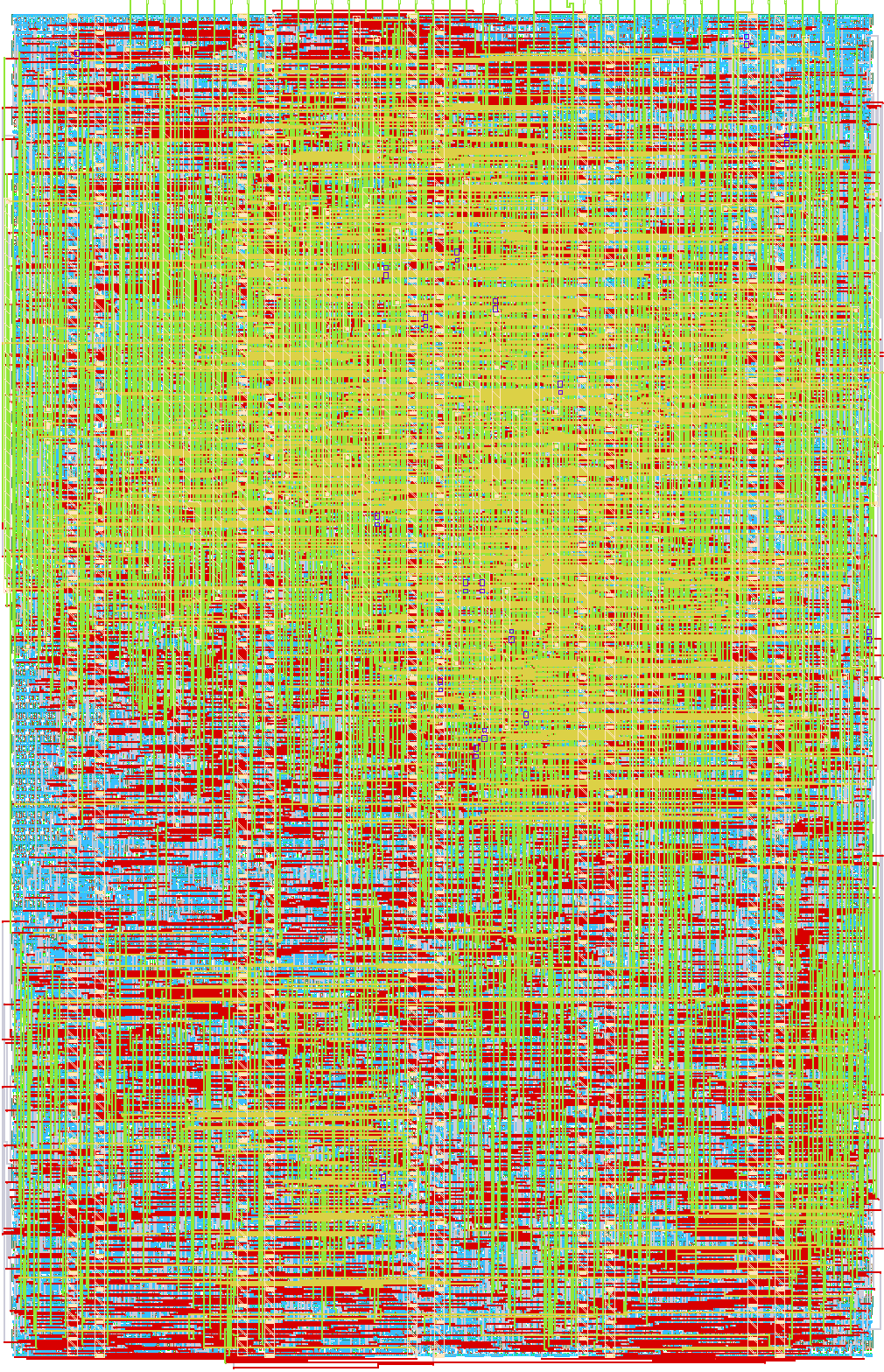
- Author: Fabien
- Description: General-purpose programmable IO prototype; not ready for tapeout
- GitHub repository
- Open in 3D viewer
- Open in Tiny Tapeout Explorer
- Clock: 50000000 Hz
AstraPIO — single PIO plus timed I/O (ABI v5)
Branch warning: this development revision adds a configurable
timed pulse-I/O engine beside one general-purpose PIO context. It is not physically
qualified or submitted. The already submitted compact fallback is commit
946648ff / shuttle PR 142, whose central checks passed. Its results do not
qualify this extension. See docs/dense-pio-v5.md for the architecture,
migration, tests and limitations.
Experimental general-purpose programmable digital IO coprocessor, not yet qualified for fabrication. This is ABI 0x0500; earlier single/dual-context and SRAM submissions describe different implementations.
How it works
One interpreter uses a programmable 16-word, 10-bit instruction store made from IHP standard-cell latches, with two-byte transmit and receive queues. One instruction slot occurs every four chip clocks. There is no SRAM macro. An autonomous pulse engine can concurrently capture a 1..24-bit prefix, replace it on a regenerated output stream and relay subsequent bits. Timing and routing are programmable; WS2812B V5 is one tested profile, not a hardwired ASIC purpose.
The host uses SPI mode 0, MSB first: command byte (02 write / 03 read), register address byte, then a 16-bit payload. Program words occupy the low ten bits; upper bits must be zero. Stop the interpreter before changing its program. Probe identity 5049, ABI 0500 and context count 1 before using the driver. SPI high/low periods and CS setup/hold/gap each require at least six ASIC clocks. MISO is not tri-stated.
How to test
Reset, confirm ID/ABI/context count/capacity registers (00/01/02/0F), load and read back code, set entry PC and GPIO mask, then run with mask 1. Use assembler option --abi 5; old binaries are incompatible. The pin-level suite checks program integrity, 14 output indices, FIFO/SPI atomicity, UART timing, faults and reset, plus pulse-stream capture/replacement/relay while the interpreter runs independently.
See docs/dense-pio-v5.md for the register map, ISA migration and verification scope. Pulse timing must be configured for the actual attached device. No broad WS2812 compatibility or physical timing qualification is claimed at this development stage.
External hardware
A host MCU (intended LPC546xx), clock source and wiring for the selected programmable protocol. The exact LPC546xx board transport/DMA and board timing remain to be qualified. No external memory is required for the compact examples.
Pin use
ui0/1/2: host SCK/MOSI/CS_n; ui3..7: five dedicated PIO inputs.
uo0/1: MISO/IRQ; uo2..7: six dedicated PIO outputs.
uio0..7: eight bidirectional PIO pins. The single interpreter may own any of the 14 outputs; the pulse engine exclusively owns at most one. Masks cannot overlap. All pad output values are forced low and uio directions disabled on reset or deselection; dedicated outputs are not tri-state.
Qualification status
This branch is for development and independent CI. No SRAM waiver, DRC filtering or nonblocking signoff exception is permitted. Placement/routing, timing including latch/clock-gate paths, DRC, LVS and official precheck must all pass before a new revision can be considered.
The compact candidate at commit 946648f completed the official flow in 1×2 tiles on 2026-09-18: Magic/KLayout DRC, LVS, XOR, antenna checks, nominal-RC timing at three cell corners, ten official prechecks and ten routed functional tests passed. The latest eleven-test suite also passes locally on that exact routed netlist. That compact candidate was submitted as PR 142; this timed extension has not been submitted. Board timing review remains separate. Detailed fallback evidence is in docs/compact-validation.md.
IO
| # | Input | Output | Bidirectional |
|---|---|---|---|
| 0 | HOST_SCK | HOST_MISO | PIO_IO0 |
| 1 | HOST_MOSI | HOST_IRQ | PIO_IO1 |
| 2 | HOST_CS_N | PIO_OUT0 | PIO_IO2 |
| 3 | PIO_IN0 | PIO_OUT1 | PIO_IO3 |
| 4 | PIO_IN1 | PIO_OUT2 | PIO_IO4 |
| 5 | PIO_IN2 | PIO_OUT3 | PIO_IO5 |
| 6 | PIO_IN3 | PIO_OUT4 | PIO_IO6 |
| 7 | PIO_IN4 | PIO_OUT5 | PIO_IO7 |