546 nanoPIO
546 : nanoPIO
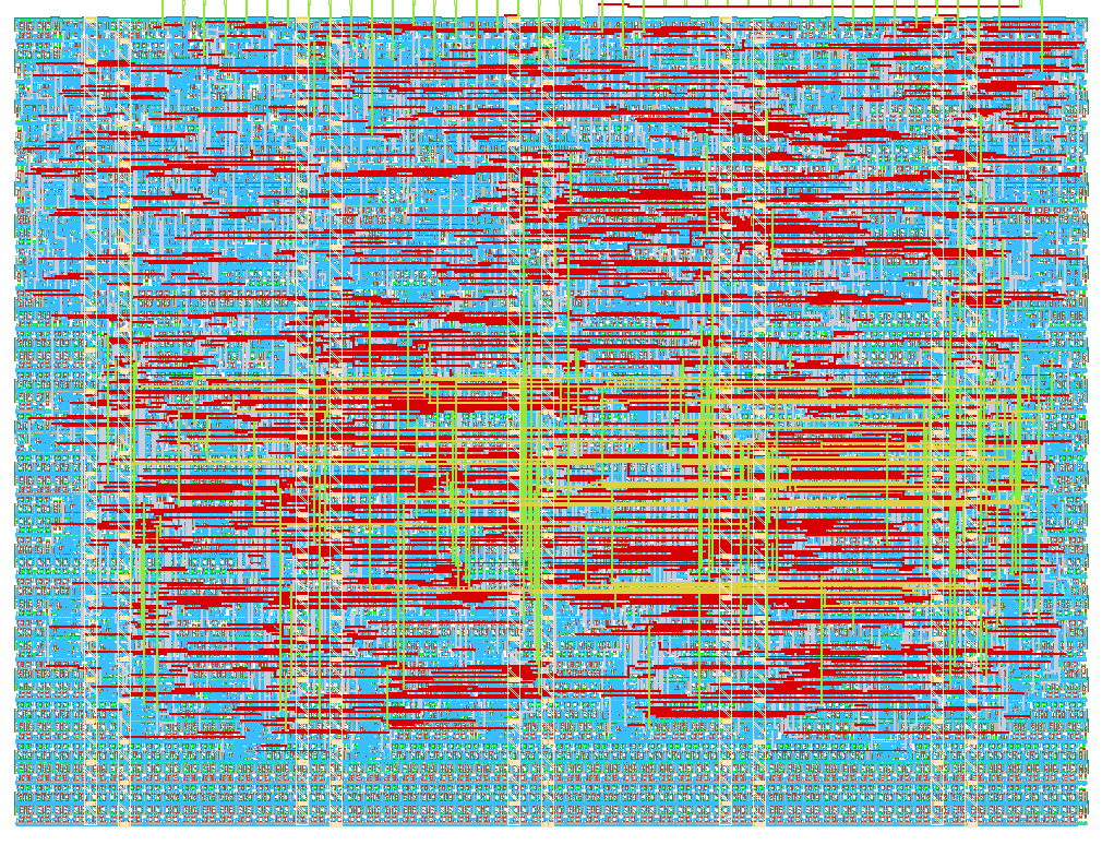
- Author: catalinlazar
- Description: A tiny bit-banged programmable I/O engine (RP2040 PIO-inspired) with a reprogrammable 16-word instruction store, used to emulate UART/SPI/I2C timing.
- GitHub repository
- Open in 3D viewer
- Open in Tiny Tapeout Explorer
- Clock: 10000000 Hz
nanoPIO — how it works
Instruction word (13 bits, 16-word program store)
[12:10] opcode
[9:7]   delay    (0-7 extra stall cycles applied after the instruction's effect)
[6:0]   operand  (meaning depends on opcode)
| opcode (3b) | mnemonic | operand layout | effect |
|---|---|---|---|
| 000 | JMP | [6:5]=cond [3:0]=addr |
PC <= addr if cond true, else PC+1 |
| 001 | WAIT | [6]=pol [2:0]=pin idx |
stall (no PC advance) until ui_in[idx] == pol |
| 010 | IN | unused | X <= ui_in |
| 011 | OUT | [6]=dest (0=uo_out,1=uio_out) |
dest <= X |
| 100 | SET | [6:0]=imm7 |
X <= {1'b0, imm7} |
| 101/110/111 | reserved | — | NOP (PC+1) |
JMP conditions
| cond (2b) | name | taken when |
|---|---|---|
| 00 | ALWAYS | always |
| 01 | X==0 (XZ) | X == 0 |
| 10 | X!=0 (XNZ) | X != 0 |
| 11 | DEC | X != 0 (checked before decrement); X is then decremented regardless of branch direction |
DEC is the classic PIO loop primitive: SET X, N then a body ending in
JMP DEC, body_start counts down N times without a separate compare
instruction.
Delay field
Every instruction (except WAIT while its condition is unmet) can attach 0-7
extra stall cycles after it executes. This lets protocol timing — a UART bit
period, an SPI/I2C clock half-period — be encoded directly into the program
instead of burning instruction words on busy-loops. This mirrors how RP2040
PIO folds [delay] into every instruction rather than giving it its own
opcode, which matters a lot when the whole program store is only 16 words.
Registers
- PC — 4 bits, indexes the 16-word instruction memory
- X — 8-bit scratch/loop-counter register. No separate ISR/OSR shift
registers like real PIO has:
INwrites straight intoX,OUTdrives straight out ofX. This is the single biggest area saving relative to RP2040 PIO, and it's a reasonable trade since TT'sui_in/uo_outare already 8 bits wide — there's no 32-bit-wide autopush/autopull to emulate.
There is no second (Y) counter in v0.1; nested loops (e.g. an outer
bit-count loop and an inner sample-delay loop) have to share X or be
restructured using the delay field instead of an inner loop.
Pinout
| Pin | Role while running | Role while LOAD_EN (ui_in[7]) is high |
|---|---|---|
ui_in[4:0] |
WAIT/IN pin sources | ignored |
ui_in[5] |
— | LOAD_DATA |
ui_in[6] |
— | LOAD_CLK |
ui_in[7] |
— | LOAD_EN |
uo_out[7:0] |
OUT PINS target |
— |
uio[7:0] |
OUT UIO target (output-only in v1) |
— |
Reprogramming (bit-bang loader)
The instruction memory is built from per-word latches gated by a shared write-address decoder (not flip-flops, and not a synthesized ROM), so it can be rewritten after fabrication. Latches roughly halve the per-bit storage cost vs. flip-flops on this PDK, which is what lets the 16-word store fit in a 1x1 tile. To load a program:
- Hold
ui_in[7](LOAD_EN) high. This halts the core (PC forced to 0,Xcleared) so it can't execute half-written instructions. - For each instruction word, shift a 17-bit frame MSB-first into
ui_in[5](LOAD_DATA), togglingui_in[6](LOAD_CLK) once per bit (rising-edge sampled, internally double-flopped for metastability):- bits
[16:13]— 4-bit address - bits
[12:0]— 13-bit instruction
- bits
- Frames can be sent in any order and re-sent to patch a single word;
LOAD_ENcan stay high across many frames. - Drop
LOAD_ENlow. The core resumes execution from address 0.
tools/nanopio_asm.py --frames prints the exact bit pattern for each frame
of an assembled program, in the order described above.
What's simplified vs. real RP2040 PIO (and why)
- 8-bit X instead of 32-bit ISR/OSR — TT's pin buses are 8 bits wide, so a wider shift register would mostly be padding.
- One scratch register, no Y — halves the register file; loop nesting falls back to the per-instruction delay field where possible.
- No autopush/autopull, no FIFO to the "system" side — there's no CPU on
the other end of this chip;
IN/OUTtalk directly to pins. uiois output-only in v1 — avoids the extra pin-direction control logic and instruction bits a bidirectionaluiowould need; revisit if area allows.
IO
| # | Input | Output | Bidirectional |
|---|---|---|---|
| 0 | PIO in[0] / WAIT PIN 0 source | PIO out[0] | PIO out[8] (uio, output only) |
| 1 | PIO in[1] / WAIT PIN 1 source | PIO out[1] | PIO out[9] (uio, output only) |
| 2 | PIO in[2] / WAIT PIN 2 source | PIO out[2] | PIO out[10] (uio, output only) |
| 3 | PIO in[3] / WAIT PIN 3 source | PIO out[3] | PIO out[11] (uio, output only) |
| 4 | PIO in[4] / WAIT PIN 4 source | PIO out[4] | PIO out[12] (uio, output only) |
| 5 | LOAD_DATA (reprogramming serial data in) | PIO out[5] | PIO out[13] (uio, output only) |
| 6 | LOAD_CLK (reprogramming bit clock) | PIO out[6] | PIO out[14] (uio, output only) |
| 7 | LOAD_EN (1 = reprogramming mode, core halted) | PIO out[7] | PIO out[15] (uio, output only) |