42 AION
42 : AION
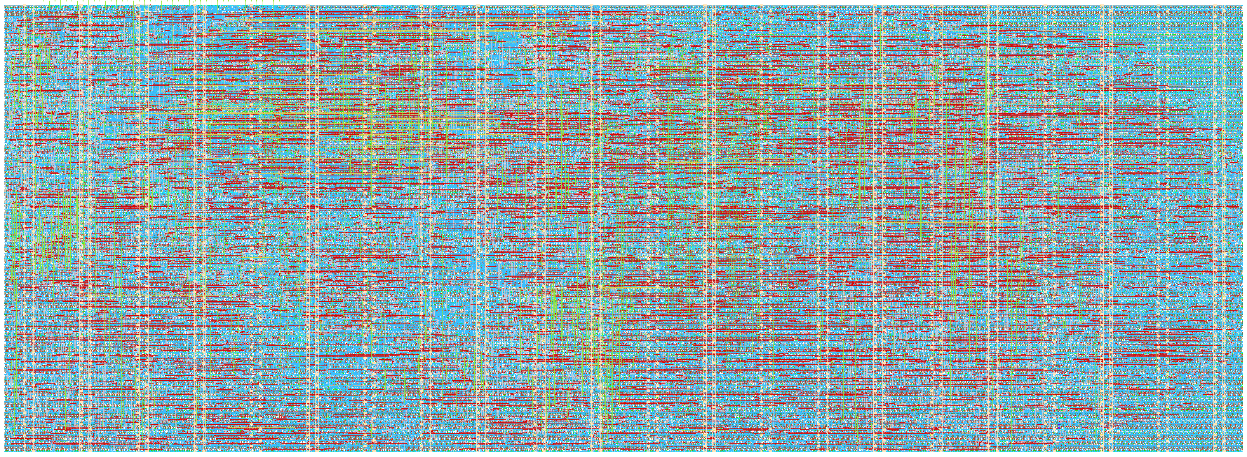
- Author: Filippo Quadri
- Description: 32-bit and 16-bit posit arithmetic unit behind a byte-wide register interface
- GitHub repository
- Open in 3D viewer
- Open in Tiny Tapeout Explorer
- Clock: 25000000 Hz
How it works
AION (AI-Optimized Netlist-to-Layout) is a posit arithmetic unit on IHP SG13G2. It adds, multiplies, compares and computes bitwise AND/OR/XOR on Posit<32,2> or Posit<16,2> numbers; the precision is chosen per command. Operands and results go through a small byte-wide register interface.
AION is a proof of concept: it tests whether AI can improve a circuit's performance by creating standard cells specific to the design, instead of using only the cells the PDK provides. Every custom standard-cell layout on this chip was drawn by an AI agent and verified with open-source tools. Besides the PDK's standard cells, the netlist uses two kinds of custom cell:
- Mined cells: pairs of PDK cells that occur often in the synthesized design, merged into single new standard cells.
- Custom logic cells: transmission-gate inverting 2:1 and 4:1 multiplexers and an inverting majority gate, which synthesis picks wherever they are smaller.
For each cell, an LLM agent wrote the program that draws the layout. Open-source tools alone decided whether it was accepted: DRC with Magic and KLayout, LVS with Netgen, parasitic extraction with Magic, timing characterization with ngspice, and a routability check with OpenROAD. The tile was then hardened with the open-source LibreLane flow (Yosys, OpenROAD, Magic, KLayout, Netgen). As a reference, the same design was also hardened with PDK cells only.
Results against the PDK-only version
Both versions use the same RTL, die, constraints (40 ns clock) and flow settings; only the cells differ.
| Metric | PDK cells only | With AION cells | Change |
|---|---|---|---|
| Standard-cell area | 121,741 µm² | 111,546 µm² | −8.4% |
| Core utilization | 46.9% | 42.9% | −3.9 pts |
| Total power (typical corner, estimated) | 129.1 mW | 99.3 mW | −23.1% |
| Routed wirelength | 406,637 µm | 359,885 µm | −11.5% |
| Setup worst slack (slow corner) | +1.87 ns | +6.90 ns | +5.03 ns |
| Hold worst slack (fast corner) | +0.150 ns | +0.138 ns | −0.011 ns |
Both versions are clean in DRC and LVS and have no setup or hold violations in any of the three corners. The tile fixes the die size, so the saved area shows up as lower utilization rather than a smaller chip. The gains come from both kinds of custom cell together.
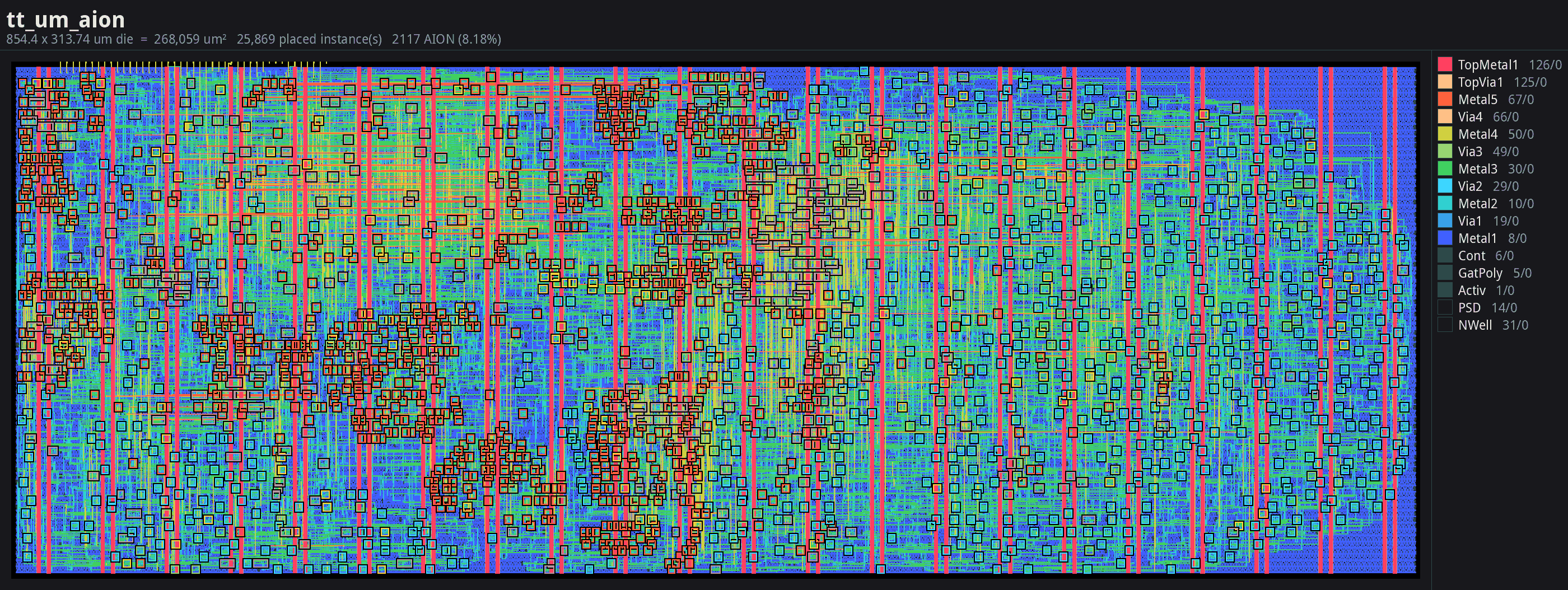
The routed 4x2 tile, coloured by metal layer; every AION cell instance is ringed.
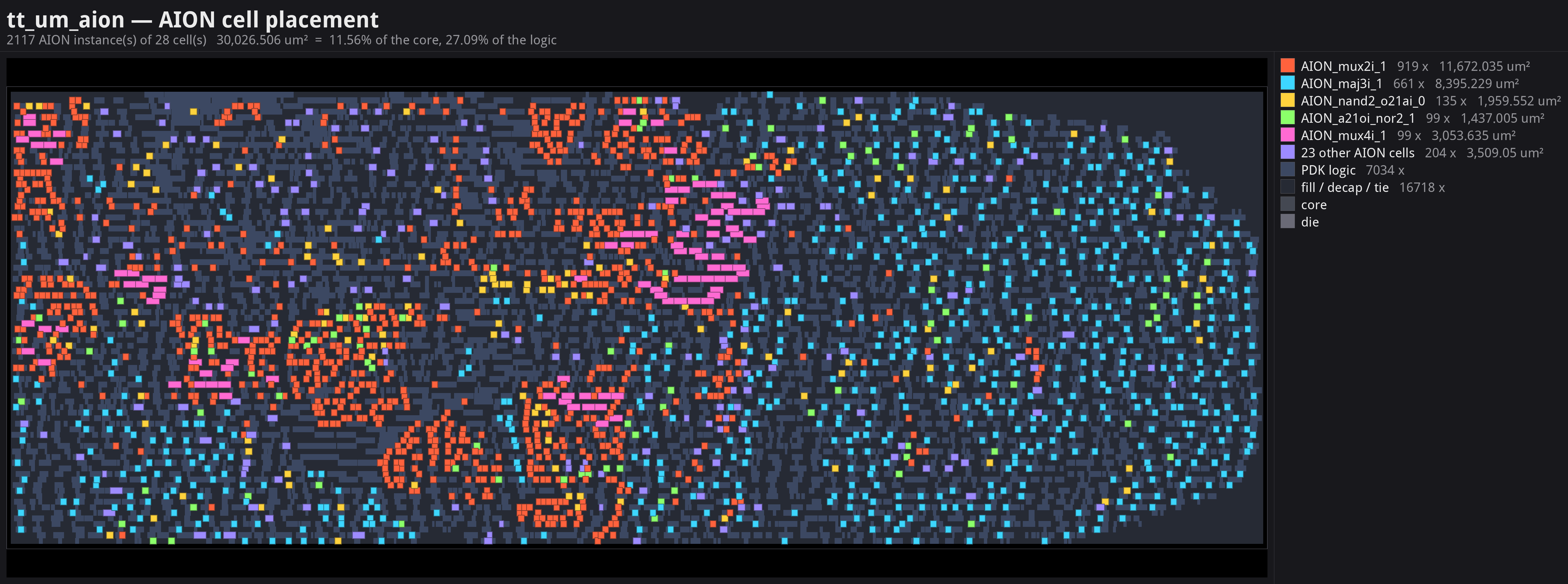
Placement map: the most-used AION cells in their own colours, the rest grouped; PDK logic and fill in grey.
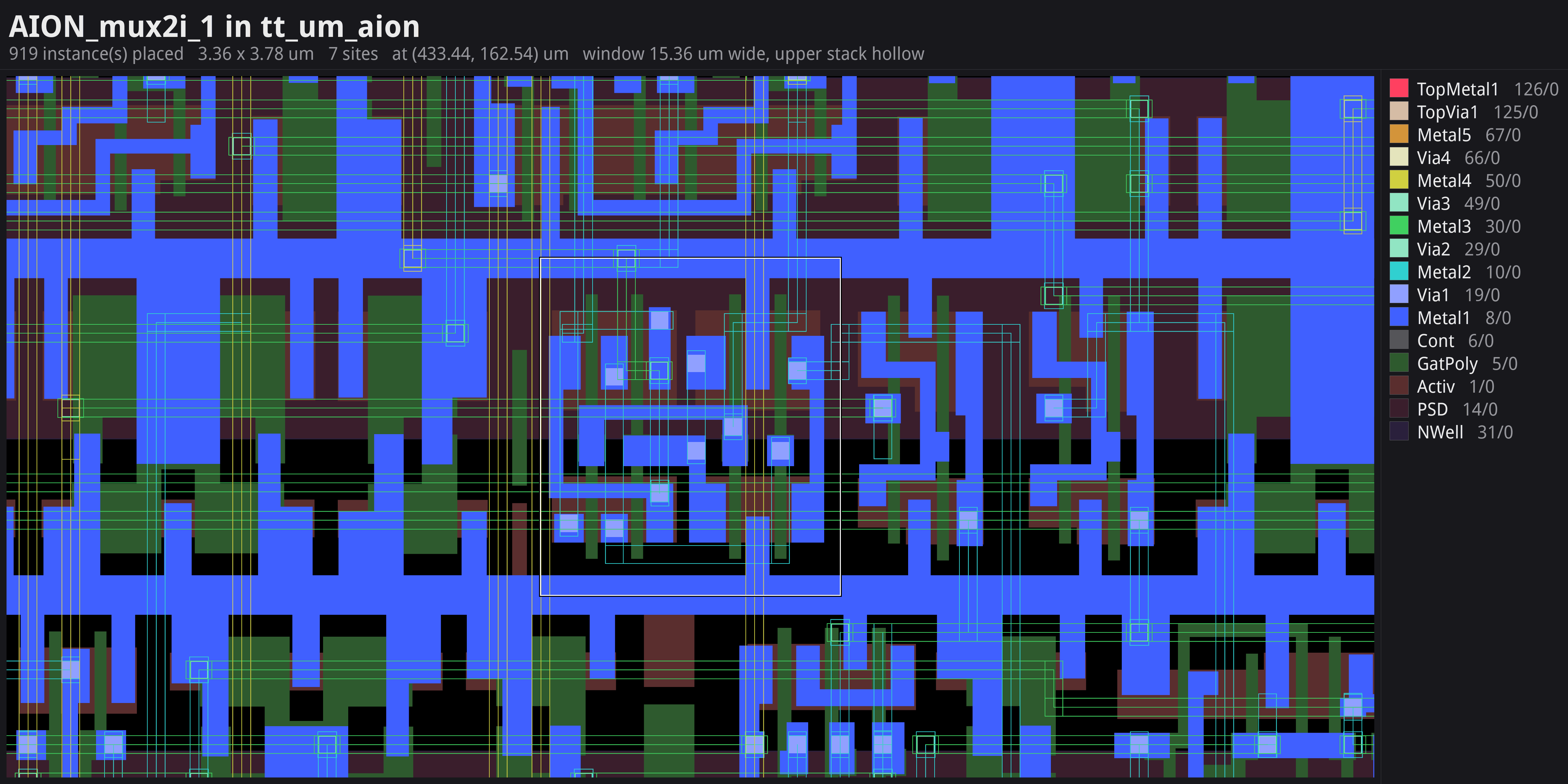
An AI-drawn transmission-gate mux (AION_mux2i_1), abutted to its PDK neighbours.
Pins
| Pin | Use |
|---|---|
ui_in[3:0] |
register address |
ui_in[7] |
1 = write, 0 = read |
uio_in[7:0] |
write data (all bidirectional pins are inputs) |
uo_out[7:0] |
read data |
Registers
| Address | Register |
|---|---|
0x0–0x3 |
operand A, low byte first |
0x4–0x7 |
operand B, low byte first |
0x8 |
control: [3:0] opcode, [4] precision (0 = 32-bit, 1 = 16-bit), [7] start |
0x9–0xC |
result, low byte first |
0xD |
status: bit 0 = done |
Opcodes: 0 add, 1 multiply, 2 equal, 3 less than, 4 AND, 5 OR, 6 XOR. Equal and
less than return a flag in bit 0 of the result. For 16-bit commands, only the low two bytes of
each operand and of the result are used.
How to test
- Hold
rst_nlow for a few clock cycles, then release it. The design is timed for a 40 ns clock period (25 MHz); any slower clock works. - Write a register: set
ui_in = 0x80 | addressanduio_in = data, then apply one rising clock edge. - Read a register: set
ui_in = addressand readuo_out(no clock edge needed). - Write both operands, then write
controlwith bit 7 set. Pollstatusuntil bit 0 is1, then read the result.doneclears whencontrolis written and is set one clock edge later.
Example: 2.0 × 3.0 in Posit<32,2>.
| Action | Value | Meaning |
|---|---|---|
write 0x0, 0x1, 0x2, 0x3 |
00, 00, 00, 48 |
A = 0x48000000 (2.0) |
write 0x4, 0x5, 0x6, 0x7 |
00, 00, 00, 4C |
B = 0x4C000000 (3.0) |
write 0x8 |
81 |
multiply, 32-bit, start |
read 0xD until bit 0 = 1 |
01 |
done |
read 0x9, 0xA, 0xB, 0xC |
00, 00, 00, 54 |
result = 0x54000000 (6.0) |
The same product in Posit<16,2>: write 00, 48 to 0x0–0x1 and 00, 4C to 0x4–0x5,
write 91 to control, and read 00, 54 from 0x9–0xA.
External hardware
None required. One 32-bit operation takes more than a dozen register writes and reads, so the practical way to drive it is a microcontroller, such as the one on the Tiny Tapeout demo board.
IO
| # | Input | Output | Bidirectional |
|---|---|---|---|
| 0 | ADDR[0] | RDATA[0] | WDATA[0] |
| 1 | ADDR[1] | RDATA[1] | WDATA[1] |
| 2 | ADDR[2] | RDATA[2] | WDATA[2] |
| 3 | ADDR[3] | RDATA[3] | WDATA[3] |
| 4 | RDATA[4] | WDATA[4] | |
| 5 | RDATA[5] | WDATA[5] | |
| 6 | RDATA[6] | WDATA[6] | |
| 7 | WRITE (1) / READ (0) | RDATA[7] | WDATA[7] |