358 PS/2 Keyboard Decoder for 68k
358 : PS/2 Keyboard Decoder for 68k
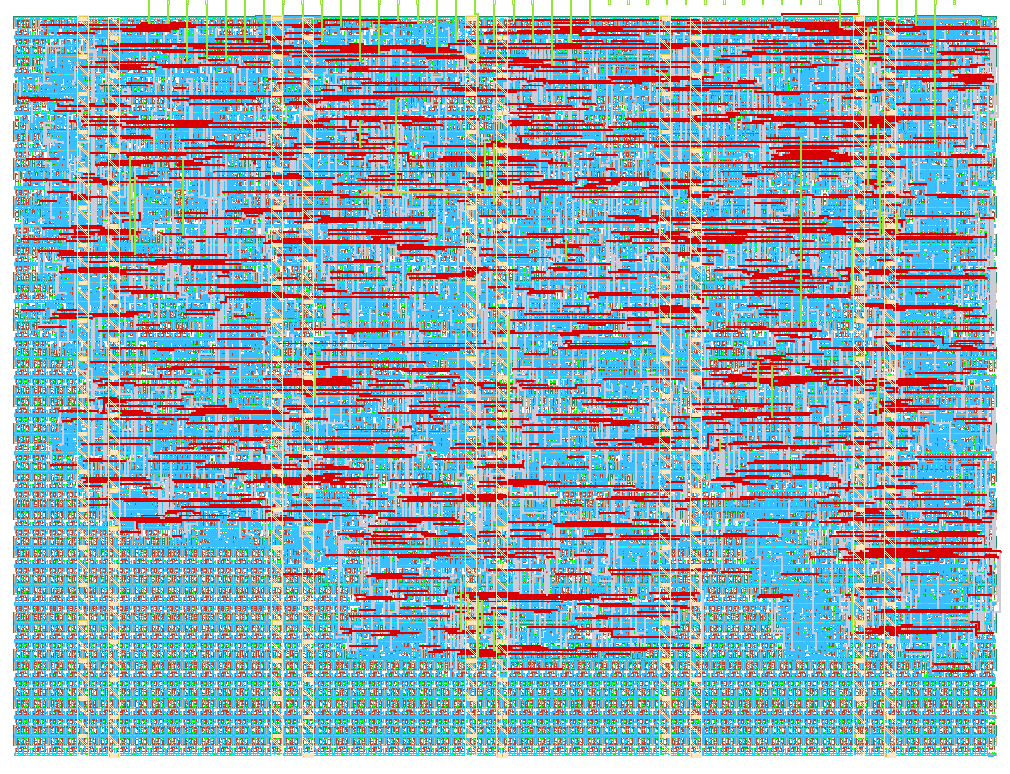
- Author: Ben Payne
- Description: A PS2 keyboard decoder for retro 68k systems (IHP SG13G2)
- GitHub repository
- Open in 3D viewer
- Open in Tiny Tapeout Explorer
- Clock: 25000000 Hz
How it works
This decoder works by first debouncing the inputs to make sure that we get a clean sample of them that is synchronized to our clock. It then looks at the down transition of ps2_clk and reads the value of ps2_data. It shifts this into a 11 bit shift register. When ps2_clk remains high for more than 1/2 of the 10kHz ps2_clk cycle it knows that the end of the data has arrived. It then triggers a valid flag to tell the system that something has arrived. The valid flag, which is exposed on a pin, will trigger the fifo to read the byte of data and it will be stored for retrieval by the host. When valid is triggered it will also trigger the interrupt pin. The valid pin is a pulse for one system clock cycle, but the interrupt will remain set until it is cleared. We also include a data_rdy signal that tells the host that there is data to read. This is useful if your interrupt handler needs to read multiple bytes.
When the host wants to read a byte, it asserts the chip select (cs) signal. The uio bus is put into an output state immediately (combinationally) whenever cs is high, and is an input bus at all other times (but we never read it...). The read itself is edge-triggered and filtered: cs and clear_int are asynchronous host signals, so both pass through a 2-flop synchronizer, and cs must then be seen high on two consecutive clocks before one byte is popped from the FIFO. Holding cs high longer never pops a second byte.
Host timing (25 MHz clock, 40 ns period):
- cs must be high for at least 2 clocks (80 ns) to register a read.
- The byte appears on the bus 5 clock edges after cs rises (synchronizer + edge detect + FIFO read register), i.e. allow at least 200 ns from cs rising before sampling the data, and keep cs high until you have sampled it. For a 68000 this means generating DTACK externally with roughly 2 wait states at 8 MHz.
- clear_int must be high for at least 2 clocks (80 ns); the interrupt drops on the 3rd clock after it rises.
- interupt is active-high; a 68k /IPL input needs an external inverter.
- valid is a single 40 ns pulse per byte - useful on a scope, not something a host should try to catch.
- These figures scale with the clock: the 128-cycle input debounce (5.1 µs) and the 100 µs end-of-frame timeout assume 25 MHz.
The design includes a fifo_full output signal that indicates when the FIFO buffer is full (4 bytes). When full, additional bytes from the keyboard will be silently dropped until space becomes available. Software should monitor this flag to detect potential data loss during rapid typing.
Interrupt semantics (important for driver writers): interupt is set by the arrival of a byte, not by FIFO occupancy. If two bytes arrive before the host services the first, reading one byte and then pulsing clear_int leaves the second byte queued with interupt low. An interrupt handler should therefore drain the FIFO while data_rdy is high (or re-check data_rdy after clear_int) rather than assume one interrupt equals one byte. Reading a byte never re-raises the interrupt; only a new arrival does.
Reading with the FIFO empty is harmless: the data bus simply holds the last byte read and the FIFO state is unchanged, so a polling host can read speculatively.
Inter-byte gap (known limitation): end-of-frame is detected by ps2_clk staying high for more than 100 µs. Two frames arriving closer together than that run together; the decoder keeps the last 11 bits, so the second byte is received and the first is lost. Real keyboards leave 1 ms or more between bytes, so this only matters for synthetic sources.
For debugging on the bench, uo[4] also carries a 115200 baud 8N1 UART transmission each time a valid byte is captured: a status byte followed by the decoded PS/2 byte. The status byte is {0000, fifo_full, data_rdy, interupt, 1} (bit 0 always 1 as a frame marker), sampled two clocks after valid so the flags reflect the byte just queued - e.g. 0x07 for a normal byte, 0x0F when it landed in a full FIFO. Bytes dropped from a full FIFO are still echoed on the UART.
Bring-up and fault isolation
A returned chip can't be repaired, so the point of the on-chip instrumentation is to work out which block failed, well enough to decide what to change on the next shuttle. Three signals that are otherwise internal are brought out on the spare output pins for that purpose:
| Pin | Signal | What it tells you |
|---|---|---|
uo[5] |
ps2_clk_dbg |
The debounced PS/2 clock, i.e. the debouncer's output |
uo[6] |
ps2_data_dbg |
The debounced PS/2 data |
uo[7] |
cs_trigger_dbg |
The internal FIFO read strobe, one clock wide per read |
They are direct taps on existing nets - no extra state, and nothing else in the design depends on them.
The reason they matter is that the UART on uo[4] reports ps2_key_data, which
is the decoder's output and therefore the FIFO's input. On its own the UART
can confirm the whole PS/2 front end works, but it can't see the FIFO's output,
and it can't distinguish a dead input pad from a debouncer that is swallowing
the signal. uo[5]/uo[6] close the first gap, uo[7] the second.
Bringing the chip up without a 68k, a keyboard, or a level shifter: nothing
requires a real keyboard - the PS/2 input is a perfectly good injection port.
Bit-bang known frames onto ui[0]/ui[1] from a microcontroller (the demo
board's RP2040 will do), and read the UART back. Because the microcontroller
drives the demo board directly, this also sidesteps the 5V level-shifting
requirement for initial bring-up. Then drive cs and sample uio from the same
microcontroller to exercise the host half.
Fault isolation table:
| Observation | Conclusion |
|---|---|
| No UART traffic at all | Clock, reset, power, or the UART block |
uo[5]/uo[6] never move while driving the PS/2 lines |
Input pad or the debouncer |
uo[5] toggles 11 times per frame but no valid |
Shift register, frame validation, or the end-of-frame timeout |
| UART fires with the right scan code | Entire PS/2 half is good, up to and including the FIFO write |
Status byte has data_rdy=0 |
Decoded correctly but the byte didn't land in the FIFO |
fifo_full asserts on the 5th byte |
FIFO counter logic is good |
UART correct but a host read returns the wrong byte, uo[7] pulsing |
cs path is fine; fault is in the FIFO read port or the uio pads |
UART correct but uo[7] never pulses |
cs synchronizer or the glitch filter |
Port from TTGF0p2 (GF180) to TT IHP 26b (IHP SG13G2)
This project was originally built for the Tiny Tapeout GF0.2µm shuttle (GlobalFoundries GF180MCU, 180nm), which offered native 5V I/O tolerance and a 3.3V core. It has been ported here to the Tiny Tapeout IHP 26b shuttle, which targets the open source IHP SG13G2 (130nm SiGe BiCMOS) PDK.
What changed:
- No VPWR/VGND ports - the IHP template's top module interface (
ui_in, uo_out, uio_in, uio_out, uio_oe, ena, clk, rst_n) doesn't require explicit power ports on every submodule, unlike the GF180 flow. All power routing is handled by the standard cell fabric. - I/O voltage - IHP's standard digital pads are not natively 5V-tolerant like GF180's. PS/2 signaling is 5V, so this design now requires external level shifting or a resistive voltage divider on
ui_in[0](ps2_clk) andui_in[1](ps2_data) to bring the signal down to the IHP pad's supported input range before it reaches the chip. This is the same external hardware requirement the original Sky130-based TT08 version of this project needed - GF180's 5V tolerance was a temporary advantage that doesn't carry over to IHP. - Core logic unchanged - the PS/2 protocol decoder, debouncer, and FIFO are the same design that passed all functional tests on the GF180 target; only the power/pad interface differs.
- Host inputs synchronized - cs and clear_int now pass through 2-flop synchronizers before anything samples them (the PS/2 inputs already did). On the GF180 version the raw cs pin fanned out to three flops in the glitch filter, which on a marginal edge could disagree and silently skip a read. Read latency is 200 ns instead of 120 ns as a result.
- UART debug output fixed - the GF180 version's UART state machine advanced past its "wait for transmit to finish" check one cycle early (the UART's busy flag has a cycle of latency), so only the status byte was ever transmitted and the data byte was dropped. The three UART tests had been skipped as "timing sensitive"; un-skipping them exposed the bug. Fixed here, and the UART module now uses an asynchronous reset like the rest of the design.
How to test
Level-shift (or resistor-divide) a standard PS/2 keyboard's 5V CLK/DATA lines down to a voltage compatible with the IHP SG13G2 I/O pads, then connect them to ui_in[0] (ps2_clk) and ui_in[1] (ps2_data). At this point you can hit keys and they will be queued in the FIFO. Then interface a retro computer to the CS, interrupt and data lines to read the FIFO. This will depend on the system you're using, but note you'll need external address decoding logic and for chips like the 68000 you'll need to generate DTACK and other bus-timing signals elsewhere.
External hardware
Connect a standard PS/2 keyboard to the chip through a level shifter / voltage divider:
- PS/2 pin 1 (DATA) → level shifter → ui_in[1]
- PS/2 pin 5 (CLK) → level shifter → ui_in[0]
- PS/2 pin 3 (GND) → GND
- PS/2 pin 4 (VCC) → 5V supply (keyboard side only)
Note: Unlike the GF180 version of this project, IHP SG13G2 does not offer native 5V-tolerant I/O, so level shifting (or a simple resistive divider) is required between the keyboard and ui_in[0:1].
Interface to your microprocessor:
- Connect CS, interrupt, and data_out[7:0] signals
- Add external address decoding logic as needed
- For 68000: Generate DTACK externally based on CS timing
IO
| # | Input | Output | Bidirectional |
|---|---|---|---|
| 0 | ps2_clk | valid | data_out[0] |
| 1 | ps2_data | interupt | data_out[1] |
| 2 | clear_int | data_rdy | data_out[2] |
| 3 | cs | fifo_full | data_out[3] |
| 4 | uart_tx | data_out[4] | |
| 5 | ps2_clk_dbg | data_out[5] | |
| 6 | ps2_data_dbg | data_out[6] | |
| 7 | cs_trigger_dbg | data_out[7] |