164 ChipLab
164 : ChipLab
- Author: Jörn Hoffmann
- Description: Educational digital logic experiments
- GitHub repository
- Open in 3D viewer
- Open in Tiny Tapeout Explorer
- Clock: 50000000 Hz
ChipLab
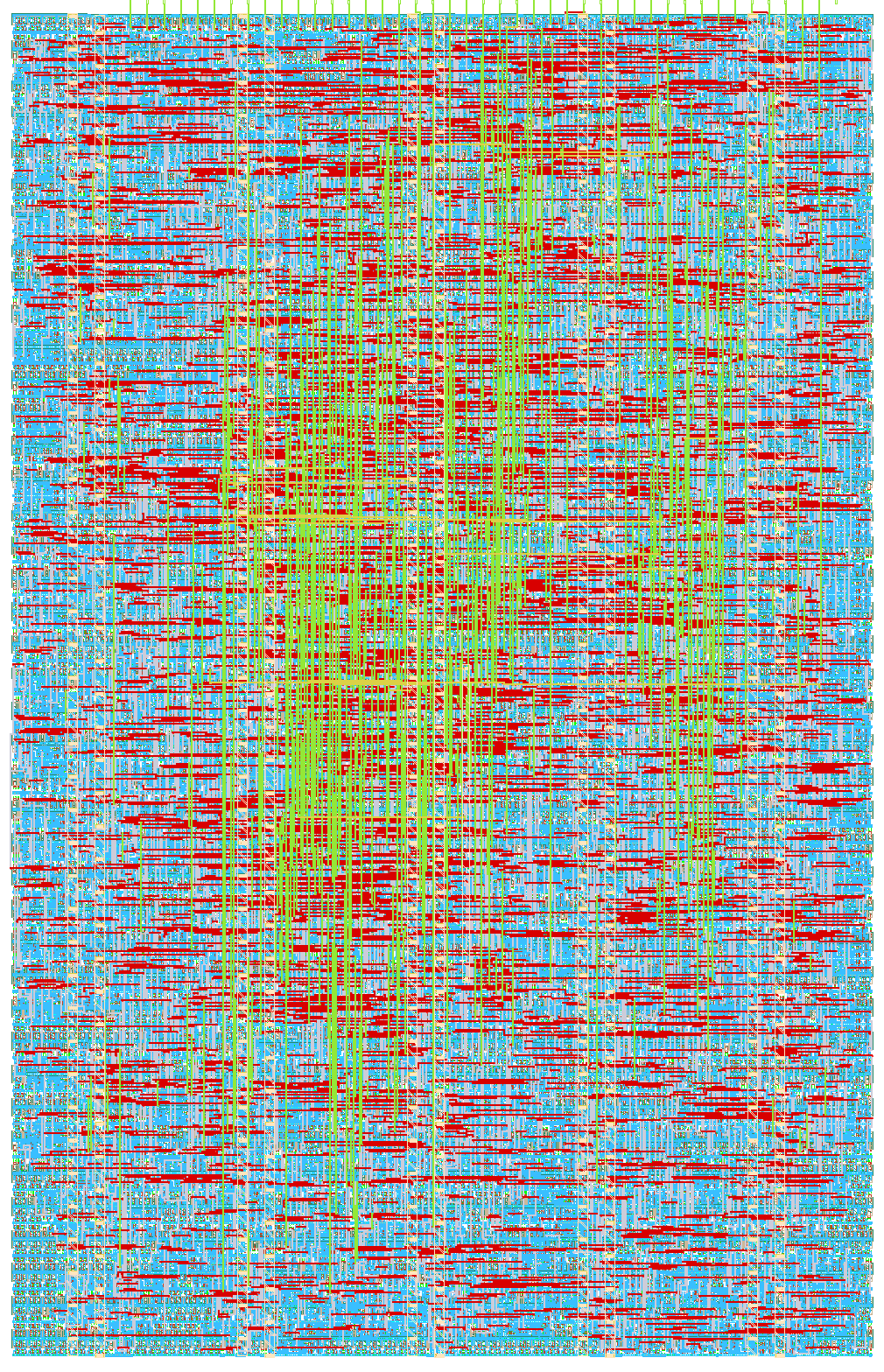
ChipLab is an educational digital logic chip for Tiny Tapeout IHP26b. Sections 1–9 are implemented, from basic logic to FSM-controlled datapaths and sound.
How it works
The design uses synthesizable SystemVerilog. uio_in[5:0] selects an experiment.
uio_in[7:6] selects an operation where needed.
All bidirectional pins are inputs (uio_oe = 0). uio_out is zero.
For experiments 1 and 2, ui_in[2:0] provides C, B, A. Higher input bits
are unused. Results appear on uo_out[7:0]. Section 2 uses the mappings below.
| No. | Selection | Experiment |
|---|---|---|
| 1. Basic and Boolean Logic | ||
| 1 | 0x01 |
Basic gates |
| 2 | 0x02 |
Boolean identities |
| 2. Data Selection and Coding | ||
| 3 | 0x03 |
Multiplexer |
| 4 | 0x04 |
Demultiplexer |
| 5 | 0x05 |
Binary decoder |
| 6 | 0x06 |
Encoder |
| 7 | 0x07 |
Priority encoder |
| 8 | 0x08 |
Dual-priority encoder |
| 9 | 0x09 |
BCD-to-7-segment decoder |
| 10 | 0x0A |
HEX-to-7-segment decoder |
| 11 | 0x0B |
Binary ↔ Gray code |
| 12 | 0x0C |
Parity generator and checker |
| 13 | 0x0D |
ROM |
| 3. Arithmetic and Data Operations | ||
| 14 | 0x0E |
Half adder |
| 15 | 0x0F |
Full adder |
| 16 | 0x10 |
4-bit adder |
| 17 | 0x11 |
4-bit subtractor |
| 18 | 0x12 |
Unsigned comparator |
| 19 | 0x13 |
Signed comparator |
| 20 | 0x14 |
Shifts |
| 21 | 0x15 |
Rotation |
| 22 | 0x16 |
ALU |
| 4. Storage Elements and Memory | ||
| 23 | 0x17 |
D latch |
| 24 | 0x18 |
D flip-flop |
| 25 | 0x19 |
T flip-flop |
| 26 | 0x1A |
JK flip-flop |
| 27 | 0x1B |
D latch and D flip-flop |
| 28 | 0x1C |
Synchronous and asynchronous reset |
| 29 | 0x1D |
Register with enable |
| 30 | 0x1E |
Register with load, hold, and clear |
| 31 | 0x1F |
4 × 4-bit read/write memory |
| 32 | 0x20 |
Accumulator |
| 33 | 0x21 |
4 × 4-bit FIFO |
| 34 | 0x22 |
4 × 4-bit stack |
| 5. Shift Registers and Counters | ||
| 35 | 0x23 |
Shift register |
| 36 | 0x24 |
Universal shift register |
| 37 | 0x25 |
Binary counter |
| 38 | 0x26 |
Up/down counter |
| 39 | 0x27 |
Modulo-6 counter |
| 40 | 0x28 |
BCD counter |
| 41 | 0x29 |
Ring counter |
| 42 | 0x2A |
Johnson counter |
| 43 | 0x2B |
LFSR |
| 6. Input Synchronization and Timing | ||
| 44 | 0x2C |
Edge detection |
| 45 | 0x2D |
Input synchronizer |
| 46 | 0x2E |
Push-button debouncer |
| 47 | 0x2F |
Clock enable divider |
| 48 | 0x30 |
PWM |
| 7. Finite State Machines | ||
| 49 | 0x31 |
Moore release control |
| 50 | 0x32 |
Mealy release control |
| 51 | 0x33 |
Traffic light controller |
| 52 | 0x34 |
Handshake controller |
| 53 | 0x35 |
Parking lot occupancy counter |
| 8. FSM-Controlled Datapaths | ||
| 54 | 0x36 |
Sequential multiplier |
| 55 | 0x37 |
Binarized neural network |
| 9. Sound | ||
| 56 | 0x38 |
Programmable sound generator |
| All other codes | All outputs zero |
Experiments 1–22 are combinational. Experiments 23–56 store state and use
clk or latch controls. rst_n resets the clocked storage elements. The two
D latches have no reset. Allow signals to settle before sampling.
| Output bit | Basic gates (0x01) |
Boolean identities (0x02) |
|---|---|---|
| 0 | NOT A | NOT (A AND B) |
| 1 | NOT B | (NOT A) OR (NOT B) |
| 2 | A AND B | NOT (A OR B) |
| 3 | A OR B | (NOT A) AND (NOT B) |
| 4 | A NAND B | A AND (B OR C) |
| 5 | A NOR B | (A AND B) OR (A AND C) |
| 6 | A XOR B | A OR (A AND B) |
| 7 | A XNOR B | A |
In the Boolean experiment, pairs (0, 1) and (2, 3) demonstrate De Morgan’s laws, (4, 5) demonstrates distributivity, and (6, 7) demonstrates absorption. Each pair has the same settled output for every input combination. Synthesis may merge equivalent logic. These experiments compare truth tables, not physical implementations or propagation delays.
Data selection and coding
Bit ranges below refer to ui_in and uo_out. Unlisted input bits are ignored.
Unlisted output bits are zero.
| Code | Input | Output |
|---|---|---|
0x03 |
Data [3:0], select [5:4] |
Selected bit on [0] |
0x04 |
Data [0], select [2:1] |
Data routed to one of [3:0] |
0x05 |
Address [2:0] |
One set bit on [7:0] |
0x06 |
One-hot data [7:0] |
Position [2:0], valid [3] |
0x07 |
Data [7:0] |
Highest position [2:0], valid [3] |
0x08 |
Data [7:0] |
Two positions and valid bits, see below |
0x09 |
BCD digit [3:0] |
Segments [6:0] |
0x0A |
HEX digit [3:0] |
Segments [6:0] |
0x0B |
Value [3:0], direction [4] |
Converted value [3:0] |
0x0C |
Data [6:0], received parity [7] |
Generated parity [0], error [1] |
0x0D |
Address [2:0] |
ROM word [7:0] |
- Encoder: exactly one set input bit is valid. Otherwise all outputs are zero.
- Priority encoder: bit 7 has highest priority. Zero input gives zero output.
- 7-segment: active-high, bits 0–6 = a–g. Bit 7 is zero (decimal point off). BCD values 10–15 blank the display. HEX letters are A, b, C, d, E, F.
- Gray: direction 0 converts binary to Gray. Direction 1 converts Gray to binary.
- Parity: even parity. Error is 1 when data plus received parity has an odd number of set bits. It detects odd numbers of bit errors, not every possible error.
- ROM: addresses 0–7 store ASCII
ChipLab\0(43 68 69 70 4C 61 62 00hex). Contents are fixed at synthesis. There is no write operation.
Dual-priority encoder (0x08)
All eight input bits are used. The circuit finds the highest set bit, clears it, and calls the same SystemVerilog function again to find the next match.
| Output | Meaning |
|---|---|
uo_out[2:0] |
Highest position |
uo_out[3] |
First match valid |
uo_out[6:4] |
Second-highest position |
uo_out[7] |
Second match valid |
Input 1011_0100 gives positions 7 and 5 (uo_out = 0xDF). Missing matches
have position zero and a cleared valid bit. The function describes combinational
logic. Its two calls do not take two clock cycles.
Arithmetic and data operations
For experiments 16–22, A = ui_in[3:0] and B = ui_in[7:4] unless noted.
| Code | Result |
|---|---|
0x0E |
Sum [0], carry [1]. Inputs are ui_in[1:0] |
0x0F |
Sum [0], carry [1]. Carry-in is ui_in[2] |
0x10 |
Sum [3:0], carry [4], signed overflow [5] |
0x11 |
Difference [3:0], no-borrow [4], signed overflow [5] |
0x12 |
Unsigned less [0], equal [1], greater [2] |
0x13 |
Signed less [0], equal [1], greater [2] |
0x14 |
Shifted value [3:0] |
0x15 |
Rotated value [3:0] |
0x16 |
Value [3:0], carry [4], overflow [5], zero [6], negative [7] |
Shift and rotation use ui_in[3:0] as value and ui_in[5:4] as amount.
For shifts, operation 0 is left, 1 is logical right, and 2 is arithmetic right.
For rotation, operation bit 0 selects left or right. ALU operations are add,
subtract, AND, and OR for operation values 0–3.
Storage elements and memory
| Code | Input | Output |
|---|---|---|
0x17 |
D [0], gate [1] |
Q [0] |
0x18 |
D [0] |
Q [0] |
0x19 |
Toggle [0] |
Q [0] |
0x1A |
J [0], K [1] |
Q [0] |
0x1B |
D [0], latch gate [1] |
Latch Q [0], flip-flop Q [1] |
0x1C |
D [0] |
Synchronous Q [0], asynchronous Q [1] |
0x1D |
Data [3:0], enable [4] |
Register [3:0] |
0x1E |
Data [3:0], control [5:4] |
Register [3:0] |
0x1F |
Data [3:0], address [5:4], write [6] |
Read data [3:0] |
0x20 |
Operand [3:0], enable [4], clear [5] |
ALU result and flags |
The D latches in 0x17 and 0x1B have an unspecified power-up value and ignore
rst_n. To initialize one on the dev kit, select its experiment, set D with
ui_in[0], then raise and lower the gate with ui_in[1] while keeping D stable.
With the gate low or the experiment deselected, the latch holds its value.
In 0x1B, reset still clears the flip-flop output.
The control values for 0x1E are hold, load, clear, and load. The accumulator
feeds its low four bits back into the same ALU used by experiment 22.
uio_in[7:6] selects add, subtract, AND, or OR.
FIFO and stack
Experiments 33 (0x21, FIFO) and 34 (0x22, stack) each store four 4-bit values.
FIFO returns the oldest entry. Stack returns the newest entry.
ui_in[3:0] supplies write data. uio_in[7:6] selects the command:
| Command | Action on a selected rising edge |
|---|---|
00 |
Hold |
01 |
Push: store the input value |
10 |
Pop: remove the next entry |
11 |
Hold (reserved) |
| Output bits | Meaning |
|---|---|
[3:0] |
Next entry. Zero when empty |
[6:4] |
Fill count (0–4). Bit [6] also indicates full |
[7] |
Empty |
Read the next entry before the pop edge. After it, the following entry appears.
The fill count is uo_out[6:4] (0–4).
Push on full and pop on empty are ignored. A held command repeats each clock.
Deselecting holds the buffer. Reset empties it even while deselected.
How to test
Shift registers and counters
Experiments 35–43 use four bits, shown on uo_out[3:0]. Bits 7–4 are zero.
They update on rising clock edges only while selected. Switching experiments
preserves their state. Active-low rst_n resets all of them asynchronously:
ring counter and LFSR start at 0001, the others at 0000.
| Code | Inputs and behavior |
|---|---|
0x23 |
Shift left. Serial input ui_in[0], enable ui_in[4] |
0x24 |
Universal shift register. Operation 0 hold, 1 left, 2 right, 3 parallel load |
0x25 |
Binary counter: 0–15, then 0 |
0x26 |
Up/down counter. ui_in[0] = 0 up, 1 down. Wraps at 0 and 15 |
0x27 |
Modulo-6 counter: 0–5, then 0 |
0x28 |
BCD counter: 0–9, then 0 |
0x29 |
Ring counter: 1, 2, 4, 8, 1 |
0x2A |
Johnson counter: 0, 1, 3, 7, 15, 14, 12, 8, 0 |
0x2B |
LFSR: left shift with XOR feedback from bits 3 and 2. 15 nonzero states |
The LFSR tap polynomial is x⁴ + x³ + 1, numbering stages 1–4
from bit 0 to bit 3. With this left-shift convention, the forward sequence
obeys s[n+4] = s[n+1] XOR s[n], whose characteristic polynomial is
the reciprocal x⁴ + x + 1. The all-zero state remains locked at zero.
Reset therefore seeds 0001.
Counters and LFSR use ui_in[4] as enable. The universal shift register uses
uio_in[7:6] as operation, ui_in[3:0] for parallel load and ui_in[0]
as serial input. Other input bits are ignored.
For example, select 0x27, set ui_in = 0x10, reset, then apply clock
pulses. The output counts 1, 2, 3, 4, 5, 0. Set ui_in = 0 to hold.
Input synchronization and timing
Experiments 44–48 update on rising edges while selected. Reset is asynchronous and active low. State holds while deselected. Unlisted output bits are zero.
| Code | Input | Output |
|---|---|---|
0x2C |
Synchronous signal [0] |
Rising pulse [0], falling pulse [1], sampled level [2] |
0x2D |
Asynchronous signal [0] |
Second synchronizer stage [0] |
0x2E |
Button [0] |
Debounced level [0], synchronized level [1], stable count [3:2] |
0x2F |
Period minus one [3:0], enable [4] |
Tick [0], counter [4:1] |
0x30 |
Duty [4:0], enable [5] |
PWM [0], phase [4:1] |
The edge detector expects an input already synchronous to the clock. It emits one pulse per sampled transition. The synchronizer uses two stages. RTL tests check their latency but cannot model metastability.
The debouncer first synchronizes the button, then accepts a changed level after four consecutive samples. Use a slow external clock for a physical button: 400 Hz gives a 10 ms confirmation window plus synchronizer latency. At 50 MHz this is only a logic demonstration, not mechanical debouncing.
The divider emits one clock-enable tick every 1–16 enabled edges. Disabling it clears the tick and holds the count. Reducing the period below the current count causes a tick on the next enabled edge. No derived clock is generated.
PWM has a 16-clock period. Duty 0 is always low. 16–31 is always high. Disabling forces the output low and holds the phase. Duty changes apply immediately, so change duty at a period boundary for clean complete periods.
State machines
Experiments 49–53 use ui_in[4] as enable. They advance only while selected
and enabled. Reset restores the initial state even while deselected.
Inputs must be synchronous to clk.
| Code | Input | Output |
|---|---|---|
0x31 |
Start [0], stop [1], enable [4] |
Moore release [0], state [1] |
0x32 |
Start [0], stop [1], request [2], enable [4] |
Mealy release [0], state [1] |
0x33 |
Phase tick [0], enable [4] |
Red [0], amber [1], green [2], state [4:3] |
0x34 |
Request [0], complete [1], enable [4] |
Ack [0], busy [1], state [3:2] |
Both controllers have two states: IDLE (0) and ACTIVE (1). Start enters ACTIVE and stop returns to IDLE on an enabled rising edge. Stop has priority if both inputs are high. Reset returns to IDLE.
Moore release is high whenever the state is ACTIVE. Mealy release is high only when the state is ACTIVE and request is high. Toggle request with the clock stopped to see the difference: the Mealy output follows immediately, while the Moore output stays high. Request is unused in the Moore experiment. Enable controls state updates only. It does not suppress either output.
The traffic light starts red (state 0). Each phase tick advances to red+amber (1), green (2), amber (3), then red. An external controller supplies the phase timing. Holding the tick high advances on every enabled edge.
The handshake starts idle (0). A request enters busy (1). Complete enters ack (2). Keep request high until ack, then lower it to return to idle. Holding request high in ack cannot start another transaction.
Parking lot occupancy counter
Select 0x35. Sensor A is ui_in[0], sensor B is ui_in[1], and enable is
ui_in[4]. Sensor value 1 means occupied. Supply synchronous sensor inputs.
- Enter: A/B =
00 → 10 → 11 → 01 → 00. - Exit: A/B =
00 → 01 → 11 → 10 → 00. - Repeated samples hold the state. Reversing follows the path back without counting.
- Skipped steps discard the crossing. Both sensors must be clear before restarting.
Output: occupancy [3:0], entered [4], exited [5], crossing/recovery active
[6], invalid-sequence recovery [7]. Occupancy saturates at 0 and 15.
The event outputs still report crossings at these limits and last one clock.
Selection and enable pause the state and count. Event pulses still clear.
Reset clears the count and returns to idle. A sensor sequence already in progress
at reset cannot reliably identify a complete crossing.
FSM-Controlled Datapaths
Sequential multiplier
Select 0x36. Inputs ui_in[3:0] and ui_in[7:4] are unsigned operands
A and B. uio_in[6] is start and uio_in[7] selects the output view:
| View | Output |
|---|---|
| 0 | 8-bit product |
| 1 | Busy [0], done [1], state [3:2], completed steps [6:4] |
States are idle (0), run (1), and done (2). Assert start for an idle clock edge to capture the operands. Four more selected edges complete the calculation. The datapath reuses two 4-bit adders from group 3. During run, operand changes and start are ignored. The product view shows the partial sum. Done holds while start is high. A selected edge with start low returns to idle, retaining the product. Deselecting pauses the calculation. Reset aborts it.
For 7 × 15, apply ui_in = 0xF7, pulse start, and wait four more edges.
The product is 105 (0x69).
Binarized neural network
Experiment 55 (0x37) implements one binary layer with eight shared input bits.
BNN_NEURON_COUNT selects 1–8 neurons at synthesis time (default: 1). A simulation
assertion rejects counts outside this range. Weights and thresholds are programmed
through registers. Training takes place outside the chip.
Each neuron compares its eight weight bits with the input using XNOR. A balanced
popcount tree counts the matching bits (0–8). Its output is one when the count is
at least the programmed threshold. Bits represent -1 and +1, so the corresponding
signed dot product is 2 * count - 8. The hardware only needs the match count.
Threshold 0 always passes. Thresholds 9–15 always fail.
uio_in[7:6] |
Action |
|---|---|
00 |
Calculate one neuron per selected rising edge, if enabled and not finished |
01 |
Latch the register address from ui_in |
10 |
Write ui_in to the selected register |
11 |
Read the selected register on uo_out |
| Address | Register | Meaning |
|---|---|---|
0x00 |
INPUT | Eight shared input bits |
0x01 |
CONTROL | Calculation enable in bit 0 |
0x02 |
OUTPUT | One result bit per neuron, read-only |
0x03 |
STATUS | Result valid in bit 0, read-only |
0x04 |
NEURON | Neuron selected for configuration and diagnostics |
0x05 |
WEIGHTS | Eight weights of the selected neuron |
0x06 |
THRESHOLD | Threshold of the selected neuron, bits 3:0 |
0x07 |
MATCHES | Live XNOR result of the selected neuron, read-only |
0x08 |
COUNT | Live match count of the selected neuron, read-only |
One shared datapath processes the neurons in ascending order. After exactly
BNN_NEURON_COUNT processing edges, STATUS becomes 1 and the complete result
holds. Other bus operations, disable, and deselection pause the calculation.
Outside read mode, uo_out shows OUTPUT. Partial results are visible before
STATUS becomes 1. Unused high result bits are zero.
Writing INPUT, WEIGHTS, or THRESHOLD clears OUTPUT and STATUS and restarts the
sequence at neuron zero. Selecting a neuron does not restart calculation.
Out-of-range neuron selections are ignored (the previous selection remains).
Writes to read-only or unused registers are ignored. Unused addresses read zero.
Reset clears the weight bank, thresholds, input, result, and enable. Diagnostics
are combinational: immediately after reset, MATCHES is 0xFF and COUNT is 8.
Example for neuron zero: program INPUT=0xB2, WEIGHTS=0xB0, THRESHOLD=7, then
enable calculation and apply the required processing edges. MATCHES is 0xFD,
COUNT is 7, and OUTPUT bit 0 is one. Program the other thresholds above 8 to
suppress their output bits.
Sound
Programmable sound generator
Experiment 56 (0x38) combines a register bank, square-wave generator, LFSR,
falling envelope, and PWM output. It has one voice with tone, noise, tone XOR noise, or tone AND noise.
uio_in[7:6] |
Action |
|---|---|
00 |
Play. No register write |
01 |
Latch the register address from ui_in on the rising edge |
10 |
Write ui_in to the selected register on the rising edge |
11 |
Read the selected register on uo_out |
| Address | Register |
|---|---|
0x00 |
Tone period, low byte |
0x01 |
Tone period, high byte |
0x02 |
Volume [3:0], 0–15 |
0x03 |
Enable [0], source [2:1] (tone, noise, XOR, AND), envelope mode [3] |
0x04 |
Envelope decay rate, 0–255 |
0x05 |
Writing bit [0] = 1 starts/restarts the envelope. Reads return zero |
0x06 |
Tone prescaler exponent [2:0], default 4 (divide by 16) |
0x07 |
Envelope prescaler exponent [2:0], default 2 (divide by 4096) |
Registers 0x06 and 0x07 are enabled by PSG_TONE_PRESCALE and
PSG_ENVELOPE_PRESCALE in the current build. If disabled, they read zero and
ignore writes, and the corresponding divider stays fixed at its default.
Unused addresses read zero and ignore writes. Unused register bits read zero.
Reset clears the sound settings, restores the default prescalers, and silences
the voice. A held write repeats on every
edge, so return to 00 after a trigger write. Period bytes are independent.
Write both while disabled for a clean note change. Each period write restarts
the tone divider and noise seed. Other writes do not stop playback.
Outside read mode the output is:
| Bits | Meaning |
|---|---|
[0] |
PWM audio |
[1] |
Selected source (tone, noise, XOR, or AND), gated by enable |
[5:2] |
Current amplitude: volume or envelope level |
[6] |
Envelope has not finished |
[7] |
Sound enabled |
With P_tone = 2^TONE_PRESCALE, the tone frequency is
f_clk / (2 * P_tone * (period + 1)). At the default divide-by-16 setting and
50 MHz, period 3550 (0x0DDE) gives about 440 Hz. The PWM carrier is
f_clk / 15. The PWM gate passes level / 15 of the phase slots, so level 15
passes the source continuously. These ratios describe the gate, not the duty
cycle of the complete audio waveform. Zero amplitude or disabled sound produces a low audio
output. Route PWM through an external low-pass filter and amplifier.
Read mode replaces the audio pins with register data. It interrupts the physical
audio output even though the generator keeps running.
Noise advances at f_clk / (P_tone * (period + 1)). The 16-bit LFSR shifts left,
XORs bits 15, 14, 12, and 3, and starts at 1. Tap polynomial:
x^16 + x^15 + x^13 + x^4 + 1, with 65535 nonzero states.
The taps follow AMD/Xilinx XAPP052, table 3.
A trigger loads the envelope from volume. With sound and envelope mode enabled,
it drops by one every P_env * (rate + 1) clocks, stopping at zero.
Here P_env = 2^(10 + ENVELOPE_PRESCALE), which defaults to 4096.
Disabling sound or envelope mode pauses decay. Changing volume does not reload
an active envelope. Deselecting the PSG pauses all its state. Reset still works.
Example at 50 MHz: write period low 0xDE, period high 0x0D, volume 0x0F,
decay rate 0xFF, control 0x09, then trigger 0x01. Return to operation 00.
This plays a roughly 440 Hz note whose amplitude falls to zero in about 0.315 s.
Basic checks
Select 0x01 and try all four combinations of A and B. Select 0x02 and try all
eight combinations of A, B, and C. Each adjacent output pair must agree.
For 0x08, test zero, a single set bit, and multiple set bits.
For example, A = 1, B = 0, C = 0 gives uo_out = 0x5A for 0x01
and uo_out = 0xC3 for 0x02.
Each experiment has its own cocotb test file. Combinational tests cover all 256 input bytes where useful. Shared tests check selection codes and experiment switching. Sequential tests provide their own clock and reset sequence. See Local Simulation for setup and commands, and Experiment Plan for the full curriculum.
External hardware
Digital switches or a controller can supply the selection and input signals. Observe outputs with a logic analyzer or an LED interface with suitable drivers and current limiting. Follow the development board’s I/O voltage requirements.
IO
| # | Input | Output | Bidirectional |
|---|---|---|---|
| 0 | Data 0 | Result 0 | Experiment select 0 |
| 1 | Data 1 | Result 1 | Experiment select 1 |
| 2 | Data 2 | Result 2 | Experiment select 2 |
| 3 | Data 3 | Result 3 | Experiment select 3 |
| 4 | Data 4 | Result 4 | Experiment select 4 |
| 5 | Data 5 | Result 5 | Experiment select 5 |
| 6 | Data 6 | Result 6 | Operation select 0 |
| 7 | Data 7 | Result 7 | Operation select 1 |