232 Ring oscillator frequency meter
232 : Ring oscillator frequency meter
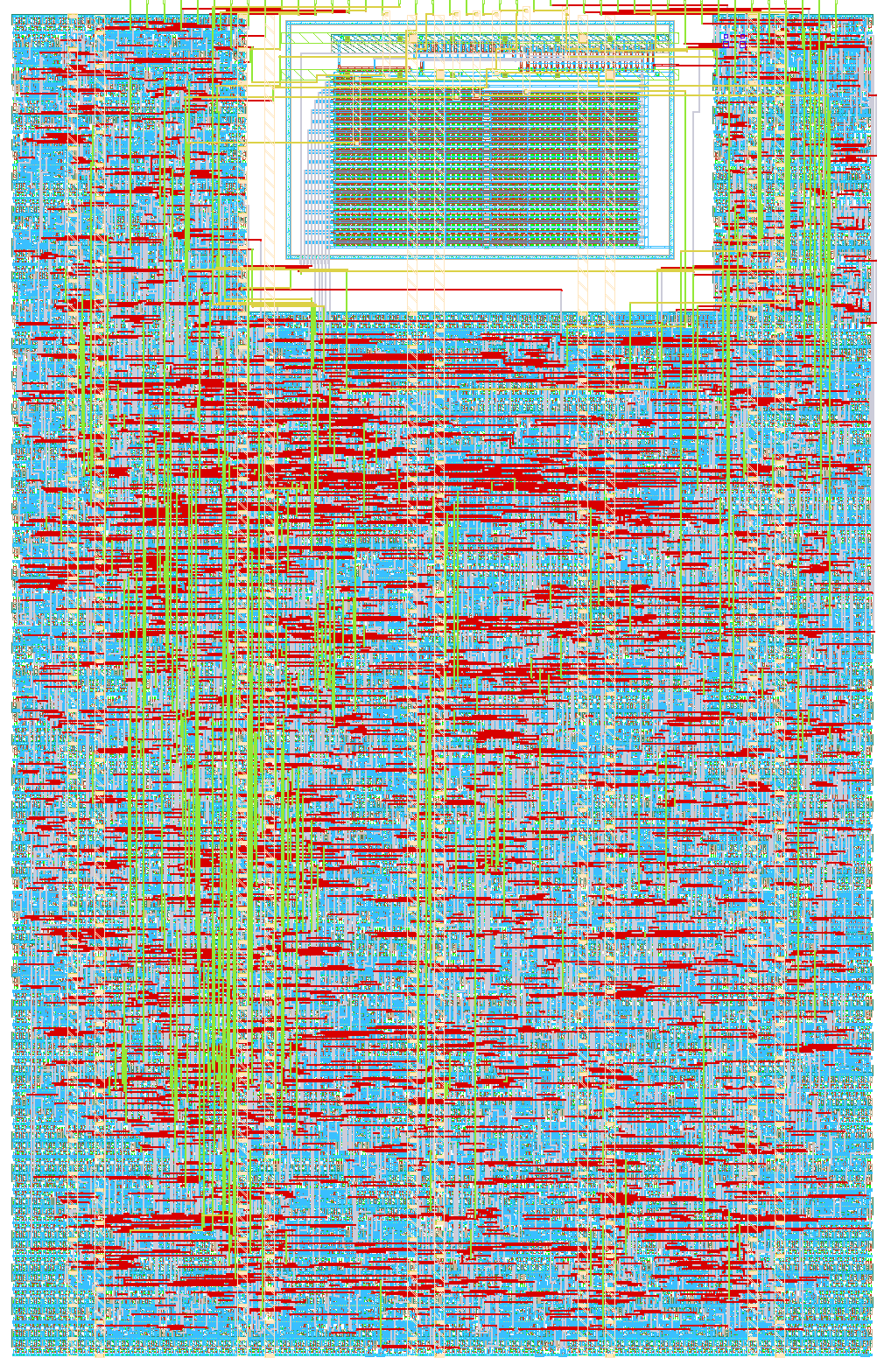
- Author: Maxwell Pauly
- Description: Reciprocal frequency counter that measures any of eight on-chip ring oscillators (incl. a trimmable one) and reports the count over the pins
- GitHub repository
- Open in 3D viewer
- Open in Tiny Tapeout Explorer
- Clock: 50000000 Hz
How it works
A reciprocal frequency counter for eight on-chip ring oscillators: it
counts reference-clock (clk) cycles inside exactly TARGET_N periods of
the selected ring, divided by 2^TAP_SEL (1..128).
f_ring = TARGET_N * 2^TAP_SEL * f_ref / RESULT
Only f_ref must be accurate, and it is a clock on a digital input. The
divider, counter, window state machine and register file are shared, so a
difference between two rings is a real difference. One 8-bit trim code is
broadcast to all rings.
| slot | ring |
|---|---|
| 0..3 | 21-stage minimum-drive, identical netlists |
| 4 | 21-stage high-drive |
| 5 | 11-stage minimum-drive |
| 6 | tap-select trimmed, 5..19 stages by code[2:0] |
| 7 | analog hard macro: 11-stage current-starved ring, 8-bit binary-weighted current DAC; 2 MHz at code 0 to 164 MHz at code 255 typical, monotonic, about 3x over PVT |
How to test
ui_in[2:0] write address, ui_in[3] write strobe, uio_in[7:0] write
data, ui_in[6:4] selects the byte on uo_out. Drive clk from an
accurate source; 50 MHz assumed below.
- Reset. Set
ui_in[6:4]= 7;uo_outmust read0xA5. - Write (address and data on the pins,
ui_in[3]high for at least 4 clocks): addr 1RING_SEL= 0, addr 2TAP_SEL= 3, addr 3/4TARGET_N= 200 (0xC8, 0x00), addr 5/6TIMEOUT= 16000 (0x80, 0x3E). - Write 1 to addr 7 (
START). - Read
STATUS(ui_in[6:4]= 0) until bit 0done. Bit 2timeout_errormeans the ring did not run. - Read
RESULTbytes withui_in[6:4]= 1..4. A 350 MHz ring gives about 229;f = 200 * 8 * 50 MHz / RESULT. - Repeat over
RING_SEL0..7 andTRIM_CODE(addr 0) 0..255. - Optional, statistics: repeat step 3..4 N times without changing any
register, then set
ui_in[7]= 1, put an index onuio_in[4:0], and readuo_out: 0..1COUNT, 2..3MIN, 4..5MAX, 6..9SUMofRESULT(little-endian) since the last register write.SUM / COUNTis the average,MAX - MINthe peak-to-peak spread. Index 10 is a random byte, 11 reads0x5A, 12..25 spell a message.
Rules:
- The divided ring must stay below 250 MHz.
TAP_SEL= 3 is safe for every ring at every corner; 2 suffices below 1 GHz. - Slot 7 at code 0 is about 2 MHz: 200 periods through tap 3 take 800 us,
longer than 16000 cycles at 50 MHz. Use tap 0 or 1 for low codes, or
raise
TIMEOUT(max 65535 cycles, 1.3 ms). - Change the code only between measurements.
Register map, pin map and sweep script: docs/ and scripts/ in the
repository.
External hardware
An accurate clock on clk (the demo board's for bring-up, a lab source
for characterisation). A microcontroller or the demo board's RP2040 to run
the sweep.
IO
| # | Input | Output | Bidirectional |
|---|---|---|---|
| 0 | ADDR[0] - write address | RDATA[0] - byte selected by RSEL | WDATA[0] - write data (input) |
| 1 | ADDR[1] - write address | RDATA[1] - byte selected by RSEL | WDATA[1] - write data (input) |
| 2 | ADDR[2] - write address | RDATA[2] - byte selected by RSEL | WDATA[2] - write data (input) |
| 3 | WE - write strobe, rising edge writes WDATA to ADDR | RDATA[3] - byte selected by RSEL | WDATA[3] - write data (input) |
| 4 | RSEL[0] - read select | RDATA[4] - byte selected by RSEL | WDATA[4] - write data (input) |
| 5 | RSEL[1] - read select | RDATA[5] - byte selected by RSEL | WDATA[5] - write data (input) |
| 6 | RSEL[2] - read select | RDATA[6] - byte selected by RSEL | WDATA[6] - write data (input) |
| 7 | STATS - 1 shows the statistics byte indexed by uio[4:0] on uo | RDATA[7] - byte selected by RSEL | WDATA[7] - write data (input) |