259 EML Fabric — analog exp/ln compute cells
259 : EML Fabric — analog exp/ln compute cells
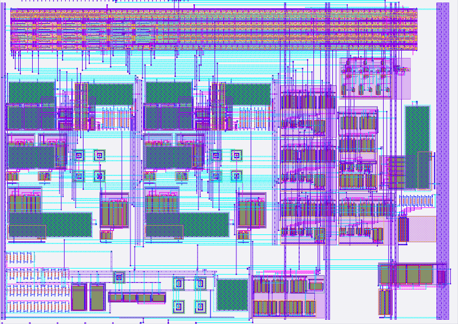
- Author: Christof Teuscher
- Description: Reconfigurable translinear EML cells (exp(u)-ln(v)): 3-cell thermistor-linearizer chain + test cell, PTAT-biased
- GitHub repository
- Open in 3D viewer
- Open in Tiny Tapeout Explorer
- Clock: 10000000 Hz
How it works
This is an analog computing tile: a chain of two EML cells, each
computing exp(u) − ln(v) in current mode using translinear NPN loops
(the "single operator" of Odrzywołek's EML formulation). Weighted
connections between cells are radix-4, all-unit-device current MDACs
(4 magnitude bits + sign per weight), and the whole fabric is biased from
an on-chip PTAT core with a 3-bit trimmed reference resistor.
The chain is x_in → CELL A → γ weight → CELL B → out_CELLB. Only the
final output is observable: with three analog pins there is no room for
stage taps, so a wrong answer cannot be localised to CELL A, the coupling
or CELL B.
Block diagram
              ua[1] iref_in
                 │  (optional external bias override)
                 ▼
        ┌──────────────────┐        ┌──────────────┐
        │  PTAT bias core  │──pbias─┤ rptat_trim   │  3-bit R trim
        │  + refchain      │        │ 15–50 kΩ     │  bits [27:25]
        └────────┬─────────┘        └──────────────┘
                 │ pbias / vcasc / vg / vg4  (to everything below)
                 ▼
 ua[0]      ┌─────────┐   out_A   ┌────────┐   ┌────────┐  sum_Bv  ┌─────────┐
 x_in ─────►│ CELL A  ├──────────►│ glue   ├──►│ γ MDAC ├─────────►│ CELL B  ├──► ua[2]
            │ exp−ln  │           │ pedestal│   │ weight │          │ exp−ln  │   out_CELLB
            └────▲────┘           └────────┘   └────▲───┘          └────▲────┘
                 │                                  │                   │
              A.u A.v                             B.γ                B.u B.v
                 │                                  │                   │
            ┌────┴──────────────────────────────────┴───────────────────┴────┐
            │   cfgdig — 29-bit scan chain, 5 weights × (4 mag + sign)        │
            └────────────────────────────────────────────────────────────────┘
                 ▲              ▲                ▲
              ui[0]          ui[2]            uo[0]
             scan_data      scan_clk          scan_out
Each cell computes eml(u,v) = exp(u) − ln(v). Every weight is a signed
radix-4 current MDAC built from identical unit devices; the weights set
u and v at each cell input, and the γ weight scales the coupling from
CELL A into CELL B.
Configuration — a 29-bit scan chain (3.3 V logic, sky130_fd_sc_hvl)
| bits | function |
|---|---|
[24:0] |
five 5-bit signed weights: A.u, A.v, B.u, B.v, B.gamma |
[27:25] |
R_ptat trim (3 bits, 8 codes) |
[28] |
chain tail — appears on scan_out |
Each 5-bit weight is w[4] = sign, w[3:0] = magnitude m, value = m/4
(full scale ±3.75 unit currents). The magnitude is two base-4 digits,
binary within each digit: m = (a0 + 2·a1) + (b0 + 2·b1)/4.
The chain is latchless: the analog follows the shift register directly, so program first, then measure — values wiggle harmlessly while a word shifts.
Analog pins — currents, not voltages
| pin | net | role |
|---|---|---|
ua[0] |
x_in |
input current |
ua[1] |
iref_in |
override/augment the internal bias reference (the chip self-biases; this is for characterisation) |
ua[2] |
out_CELLB |
final output of the chain |
How to test
- Power up (1.8 V digital + 3.3 V VAPWR). Release
rst_n— the config chain resets to a safe all-zero state (all weights off). WAIT AT LEAST 10 ms BEFORE READING ANYTHING. The PTAT bias core's start-up escape path is 5.5 pA and is junction-leakage limited, so it is slow when the leakage is small: simulated at the ss corner and −40 °C the core is still in its degenerate zero-current state at 1 ms and wakes somewhere between 1 ms and 10 ms. At tt / 27 °C it is up in microseconds, so a warm bench will not show this — but a cold part read too early will look dead, and that is a measurement artefact, not a failure. Being leakage-limited, the delay does not scale with anything you can control from outside. - Shift 29 configuration bits into
ui[0](scan_data), clocked on the rising edge ofui[2](scan_clk).uo[0](scan_out) echoes the chain 29 clocks later — shift 58 clocks and compare the second 29 to verify programming.ui[2], notui[1]:ui[1]sits off the analog macro's 0.6 µm routing grid, so no via could be placed beside it. - Drive
ua[0](x_in) with the input current: unit current is 0.5 µA, useful range roughly 0.1–6.5 µA. - Measure
ua[2](out_CELLB) for the chain result. - Optionally trim the PTAT current via bits
[27:25](8 monotonic codes spanning 15–50 kΩ, ~127 % of design current; nominal at code100) and observe the effect on any output.
No clock is required beyond the scan clock you provide; the analog is continuous-time.
Known limitations
-
Weight monotonicity is likely, not guaranteed. Each radix-4 digit is binary rather than thermometer (the thermometer decoder was removed to fit the config routing), so a code step at an inter-digit carry is a difference between matched devices instead of simply adding a leg. Simulated (schematic level): nominal DNL −0.139/+0.057 LSB; across 70 mismatch samples 0 were non-monotonic, with the per-sample worst DNL distributed mean −0.276, σ 0.190 LSB, worst observed −0.981 against the −1.0 limit. That puts the limit ~3.8σ out — but note −0.981 turned up once in 70 samples where a Gaussian at that σ predicts nearer 1 in 3800, so the tail is heavier than normal and 70 samples cannot resolve it. The margin is real but not large. If weight sweeps show a flat or reversed step, suspect codes 4, 8, 12 of a digit pair before suspecting your setup.
-
The exp term is correct as of this build:
exp(0.967·u). An earlier build computedexp(1.23·u)because the poly resistors were sized byL/W × rsheet, which ignores end resistance (~24 % low). Corrected. Measured 2026-08-14 on the layout-matched netlist (emlcell_b_sim12.inc), tt, 27 °C,u = −1 … +1.25,vheld at 1:io = 1.101 · exp(0.967·u) − 0.009 max residual 0.0004 unitsIt is a clean exponential — the residual is four ten-thousandths of a unit. The coefficient drifts slightly across the range (0.931 at
u = +0.6to 0.955 atu = −1.25), so it is not perfectly pure, but close. Earlier revisions quoted 0.96; that came from a schematic bench and was ~3.5 % optimistic. 0.927 is the die figure. -
THE ln ARGUMENT IS NOT
v. The cell computesln(v + 2.57)up to scale. Measured 2026-08-14 on the layout-matched netlist (emlcell_b_sim12.inc, derived fromlvsref/emlcell_b_flat.spice, which LVS-matches the shipped layout), tt, 27 °C, overv = 0.5 … 4:fitted against result max residual ln(v + 2.55)2.478 − 1.094·ln(v + 2.547)0.0002 units ln(v)1.05 − 0.42·ln(v)0.078 units Read the first row: as a log amplifier the cell is close to ideal — slope −1.094 against its true argument, residual two ten-thousandths of a unit. It is only the argument that is offset.
Mechanism. The layout hard-wires a bias pedestal the schematic bench never modelled:
XLPAputs a fixed 936 nA (1.872 units) on thenvtransdiode, and the reference legXLPB_LVRcarries 1394 nA (2.789 units). That accounts for roughly 1.87 units of offset. The measured offset on the shipping (unbuffered) cell is 2.57, so the pedestal explains most but not all of it; the remaining ~0.7 units is not yet accounted for and is an open item. The pedestal model was validated against the buffered build, where it matched the local slope at every point; it has not been re-fitted for this one. What is directly measured, and what should be relied on, is the fit in the table above.How to use it. Pre-map the input as
v_ext = a·v_eff − 2.57(units of the 0.5 µA reference;ais absorbed by the compiler's alpha). This has to happen in the compiler or the drive electronics:ln(v + 2.57)is notk·ln(v)for anyk, so no output gain or offset trim recovers it.silicon/README.md:158records this as the original design intent — "ln input becomes ln((v+2)/3); constants absorbed by alpha/compiler" — it simply was never carried into this document.CORRECTION. Earlier revisions of this file claimed
1.06 − 1.05·ln(v)with a 0.019-unit residual and a usable range of|error| < 0.05forv ≥ 1. All three claims were wrong. That figure came from a schematic bench (char/_v2d_lay2.inc) which (a) omits the pedestal legs the layout generates internally, and (b) is byte-identical tochar/_v2d_quiet.incand self-oscillates, so the number was read off a DC equilibrium the bench does not occupy. Time-averaging that bench through its limit cycle gives0.83 − 1.38·ln(v)with a 0.53-unit residual. The statement that the slope only collapses belowv ≈ 0.35was also wrong: without the input mapping the apparent slope varies continuously across the whole range, −0.15 atv = 0.35to −0.63 atv = 4, never reaching −1.A source-follower buffer was briefly shipped and has been REVERTED. Between 2026-08-13 and 2026-08-14 this repository carried a build with a source follower (
MSF, W16 L1) plus a 0.5 µA sink (MBM, W4 L8) added to the two ln servos, intended to fix an apparent slope error. That apparent error was an artifact of fitting againstln(v)instead of the true argument — the unbuffered cell was already a clean logarithm — and the buffer made the servo loop unstable: a sustained ~7.2 MHz limit cycle from the DC operating point with no stimulus, 1.37 units peak-to-peak at the output forv = 1(126 % of the signal), confirmed under both trapezoidal and Gear-2 integration and by active perturbation. Reverting either added device restores 0.00000 units of ripple with the DC law unchanged. The current GDS is the unbuffered cell and is stable.RESISTOR SEGMENTATION — why these differ from earlier revisions by ~4 %. The layout draws
RUandRLNas FOUR series bodies ofL = 11.44 µm; the simulation netlists and LVS references lump each as a singleL = 45.76 µmdevice. Those are not the same resistor: each body carries its own ~741 Ω of end resistance, so 4 × 11.44 measures 53.75 kΩ against 51.53 kΩ for the lump, +4.31 %. Simulating the segmented form moves the ln slope −1.145 → −1.094 and the exp coefficient 0.927 → 0.967, i.e. both ~4 % CLOSER to ideal than previously published. Post-layout extraction confirms the split: parasitic R and C contribute only 0.01 % (ln) and 0.35 % (exp) at DC, so essentially all of the difference is the segmentation, not the parasitics. The corner, temperature and Monte Carlo figures below were taken on the LUMPED netlist and carry the same ~4 % systematic; their spreads and trends are unaffected. -
Per-cell output level varies by 24 % (1 sigma). This is the accuracy floor. 440 Monte Carlo samples of the layout-matched netlist (
tt_mmplus the four skew corners), measuringioatv = 1, u = 0:mean 1.098 units, sigma 0.266 units = 24.3 % observed range 0.446 .. 1.838 units over 440 samplesThe peak-to-peak spread is 1.27x the nominal output itself. It is mismatch-limited, not process-limited —
tt_mmalone produces the full 24.3 % and the skew corners add nothing — so it will not average out across the fabric: every cell draws independently. The shape is unaffected: under full mismatch the log and antilog fits still hold to ~2.5e-4 and ~3.2e-4 units respectively. Mismatch translates the curve without bending it. So a cell remains an excellent log amplifier with an uncertain gain and offset. Consequence: treat every cell output as needing per-cell calibration. Using a raw cell output as a quantitative value carries ~24 % 1-sigma error. This cannot be trimmed out in the current silicon (it is set by device area in the level-setting legs) and it is not a corner or binning issue. -
Useful temperature window is roughly −8 °C to +54 °C. The cell has no thermal-voltage compensation, so its scale factor tracks absolute temperature by construction:
k_lnis PTAT (measured, it tracksk_ln(27 °C)·T/300 Kto within 0.6 % at every temperature from −40 to +125 °C) and the exp coefficient is the reciprocal, ~1/T. Measuredk_lnruns 0.887 at −40 °C through 1.151 at 27 °C to 1.520 at +125 °C — a 72 % swing, of which only 0.54 % is process. This is what an uncompensated bipolar translinear pair does; it is a design limit, not a defect. Because the drift is thermal rather than process, guardbanding or binning does not help — only a PTAT-referenced gain trim or a temperature-tracking reference would. The exp path binds the window. -
Stability: verified across the full box. Zero-stimulus transients from the DC operating point show
i(VOUT)peak-to-peak = 0.000e+00 at all 25 corner × temperature conditions and in all 440 Monte Carlo samples. Worst fit residual anywhere in the corner matrix is 6.6e-4 units. (An earlier build with a source-follower buffer oscillated at ~7.2 MHz and was reverted — see the note further down.) -
The on-chip bias core delivers a usable current everywhere measured, and needs no trimming to do it. Simulated on netlists derived from the shipped LVS references: nominal output 476.5 nA = 0.953 cell units (−4.7 %) at tt / 27 °C / 3.3 V / trim code 100. Supply sensitivity 0.11 %/%. Mismatch over 200 samples: sigma 1.75 %, range 0.902…1.000 units, 0 of 200 outside the ±30 % window that keeps the full input range usable — counted, not extrapolated from a sigma. The 3-bit trim is monotonic in 100 % of 9 corners × 3 temperatures × 8 codes and in 200/200 mismatch samples, spanning 15.44–50.24 kΩ (×2.95, ~17.5 %/code); a single code covers every corner at every temperature. The two PTAT effects cancel rather than compound. The cell wants
vt/RUand the core deliversvt·ln8/R_ptat— bothvt/Rin the same poly resistor material — so the resistor corner cancels to ~1 %. The delivered/wanted ratio is 0.990 at tt / 27 °C and moves only 2.27 % across −40…+125 °C, spanning 0.873…1.054 over all 27 corner × temperature combinations. The absolute current swings 2.6× across that box and looks alarming until the ratio is taken. So the temperature window above is set by the cell, not by its bias. Caveat, stated because it matters: sky130's ngspicett_mmvaries MOSFETs only — the resistor models carry no statistical terms and NPN mismatch is left as an inactive comment. The 1.75 % sigma is therefore optimistic. Bounded by hand, 1 mV of Vbe offset between the core's mirror pair is worth 1.9 % of current, and 1 % on R_ptat is worth 1.08 %. A separate systematic: the core's mirror pair sees 1.3 V of uncascoded Vds asymmetry and runs 3.07 % apart, so the loop solvesln(8.25)rather thanln(8)— about +3.7 % of current, with a further −3.3 % spread across consumer drain voltages from 0.4 to 2.0 V. -
Bias-current tolerance is the tightest operating constraint. The reference current sets BOTH transfer coefficients — they are properties of the bias, not of the topology. Scaling the whole bias generator gives
expcoefficientB = 1.853 x I[uA], constant to 0.5 %, with the ln slope moving inversely. Measured on the layout-matched netlist at tt / 27 C, varyingpbiasalone:pbias ln slope k usable v range 0.25 uA -1.309 0.25 … ≈1.8 0.35 uA -1.215 0.25 … ≈3.4 0.50 uA (nominal) -1.151 full 0.25 … 4 0.70 uA -1.115 full 1.00 uA -1.094 full, residual 19x better A −30 % bias error already clips the top of the input range — the output crosses zero at v ≈ 3.4 and goes negative beyond it. Nominal 0.5 uA sits at the LOW EDGE of the range that keeps the full v span usable. Above nominal the log conformance actually improves (max residual 1.8e-5 units at 1 uA), at the cost of DC level and MDAC headroom. This is what the 3-bit R_ptat trim (bits
[27:25]) is for; use it. -
Output loading: only DC compliance and bandwidth, never stability.
outis the drain of three devices and the gate or source of none, so it sits outside every feedback loop and a load cannot move a loop pole. MeasuredR_out= 7.1 MΩ,C_self≈ 24–40 fF; |Zout| is a single non-peaking pole for every load tested up to 100 nF.- Resistive:
v(out) = 0.9 V + io·R_L. At ≤ 100 kΩ the cost is ≤ 1.5 % on the ln slope; at 1 MΩ the node reaches 1.38 V and costs 12.7 %. - Capacitive: sets the output pole at
1/(2π·7.1 MΩ·C_L)— 22 kHz at 1 pF, 2.6 kHz at 10 pF, ~22 Hz at 1 nF. DC is untouched. No load, supply, reference or bias condition in 43 tested destabilised the cell.
- Resistive:
-
PSRR is 0.113 units/V (56.5 nA/V), flat to ~10 kHz. That is ~10 % of the DC output per volt, i.e. ~1 % per 100 mV of supply ripple. It degrades above 10 kHz: x3.6 at 1 MHz and x22 at 10 MHz, still rising. Supply sensitivity of the transfer itself is small — over 3.0–3.6 V the ln slope moves 0.21 % and the DC level +6.4 %. Both references are far less critical: ±10 % on
vrefbmoves the slope 0.08 %, and ±10 % onveleaves it unchanged to four decimals. -
The thermistor-linearisation figure has not been re-validated. The "residual 1.1 % of span" result was obtained with the earlier three-digit thermometer weight; this build has two digits, binary.
-
All results quoted here are simulation, schematic-level except where stated. Nothing has been measured on silicon.
External hardware
A source-measure unit (or one current source + one current meter) for the analog pins. Everything else — bias, references, configuration — is on-chip.
Reference
The operator this fabric implements:
A. Odrzywołek, "All elementary functions from a single operator", Institute of Theoretical Physics, Jagiellonian University, Kraków. arXiv:2603.21852v2 [cs.SC], 4 Apr 2026.
The paper shows that the single binary operator
eml(x, y) = exp(x) − ln(y)
together with the constant 1 generates the standard scientific-calculator
repertoire — constants (e, π, i), arithmetic (+ − × /,
exponentiation) and the transcendental and algebraic functions. For
example eˣ = eml(x, 1) and ln x = eml(1, eml(eml(1, x), 1)). Every
expression becomes a binary tree of identical nodes under the grammar
S → 1 | eml(S, S).
This chip is a hardware realisation of that node: two eml cells with
programmable weights, so a depth-2 tree can be evaluated in continuous
time rather than symbolically.
IO
| # | Input | Output | Bidirectional |
|---|---|---|---|
| 0 | scan_data | scan_out (readback) | |
| 1 | |||
| 2 | scan_clk | ||
| 3 | |||
| 4 | |||
| 5 | |||
| 6 | |||
| 7 |
Analog pins
ua | PCB Pin | Internal index | Description |
|---|---|---|---|
| 0 | W | 7 | x_in (analog input current) |
| 1 | T | 9 | iref_in (external bias reference) |
| 2 | U | 8 | out_CELLB (analog output of the second EML cell) |