975 ttsky26c-202607-mehmetoguzderin by Oguz
975 : ttsky26c-202607-mehmetoguzderin by Oguz
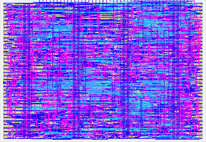
- Author: Mehmet Oguz Derin
- Description: VGA scene with flash palette, mirrored dual-PSRAM state, and two independent gamepads.
- GitHub repository
- Open in 3D viewer
- Open in Tiny Tapeout Explorer
- Open in VGA Playground
- Clock: 25175000 Hz
VGA, dual gamepad, and QSPI scene demo
Run the project at exactly 25,175,000 Hz. uo_out drives a Tiny VGA Pmod with 640×480 timing, ui_in[6:4] receives one- or two-controller Gamepad Pmod reports, and uio connects the Tiny Tapeout flash/dual-PSRAM Pmod. Populate exactly one W25Q128JVSIQ flash and two APS6404L-3SQR-SN standard-grade, non-X PSRAMs.
At startup the design resets the flash, waits at least 1,602 clocks (about 63.63 us), then reads TTD1 and a six-bit color twice. It exits either PSRAM from QPI mode, resets both devices, and tries a scene record from PSRAM B then A. Each record has a magic byte, the 20-bit scene, and a CRC-8 with polynomial 0x07; accepted or fallback state is mirrored back to both devices and verified. Missing or corrupt memories use deterministic defaults and never stall video.
The display has invariant quadrant colors, a configurable object, a wave, and memory/controller status blocks. The asynchronous Gamepad Pmod latch, clock, and data inputs pass through two-stage synchronizers; data is sampled one core clock after a synchronized gamepad-clock edge, and a report boundary waits for any pending final bit. Both SELECT buttons request a warm reinitialization without cycling Pmod power. The design first reads flash status registers 1 and 2 and refuses the reset while BUSY or SUS is set; an idle flash receives the reset-enable/reset sequence and the same recovery delay as cold startup.
Reset is synchronously captured and must be held low across a rising clock edge. Reset release passes through a two-stage synchronizer before normal operation resumes. Do not slow or manually step the clock: a paused transaction can exceed the PSRAM chip-select-low limit. Deasserting ena immediately blanks VGA and tri-states every QSPI pin; the qualified assembly must hold every CS# high while disconnected. The hard platform contract requires every selection to occur with reset active, followed by a project clock edge before reset release.
Run python3 tools/generate.py build in the devcontainer to execute the RTL test, CIRCT direct/shared equivalence and PPA selection, and regenerate src/generated.v. The GDS workflow runs hierarchy-independent cold/warm memory startup, mirrored writes, controller mutation, fallback repair, and VGA checks on the post-layout functional gate-level netlist.
Hard implementation limits are the exact Tiny Tapeout 1x1 allocation, a placement-density target no greater than 90%, and measured active instance/core utilization strictly below 90%. FPGA mapping is independently recounted and must use strictly fewer than 792 SB_LUT4 cells; equality at either exclusive limit is a failure.
Simulation and CI do not prove board behavior. An FPGA board-validation claim must bind deployment and post-reset readback of the exact bitstream to the requested clock, identified assembly/BOM, and observed interfaces such as capture-card VGA. ASIC pretapeout signoff instead relies on exact-commit logical proof, extracted physical checks, and the independent official Tiny Tapeout precheck/gate-level flow; it cannot require an ASIC board before fabrication. The complete FPGA+ASIC scope/HIL bundle is the later post-silicon release qualification.
IO
| # | Input | Output | Bidirectional |
|---|---|---|---|
| 0 | VGA R1 | QSPI flash CS# | |
| 1 | VGA G1 | QSPI MOSI / SD0 | |
| 2 | VGA B1 | QSPI MISO / SD1 | |
| 3 | VGA VSYNC | QSPI SCK | |
| 4 | Gamepad latch | VGA R0 | QSPI SD2 / WP# |
| 5 | Gamepad clock | VGA G0 | QSPI SD3 / HOLD# |
| 6 | Gamepad serial data | VGA B0 | QSPI PSRAM A CS# |
| 7 | VGA HSYNC | QSPI PSRAM B CS# |