201 quick_bus
201 : quick_bus
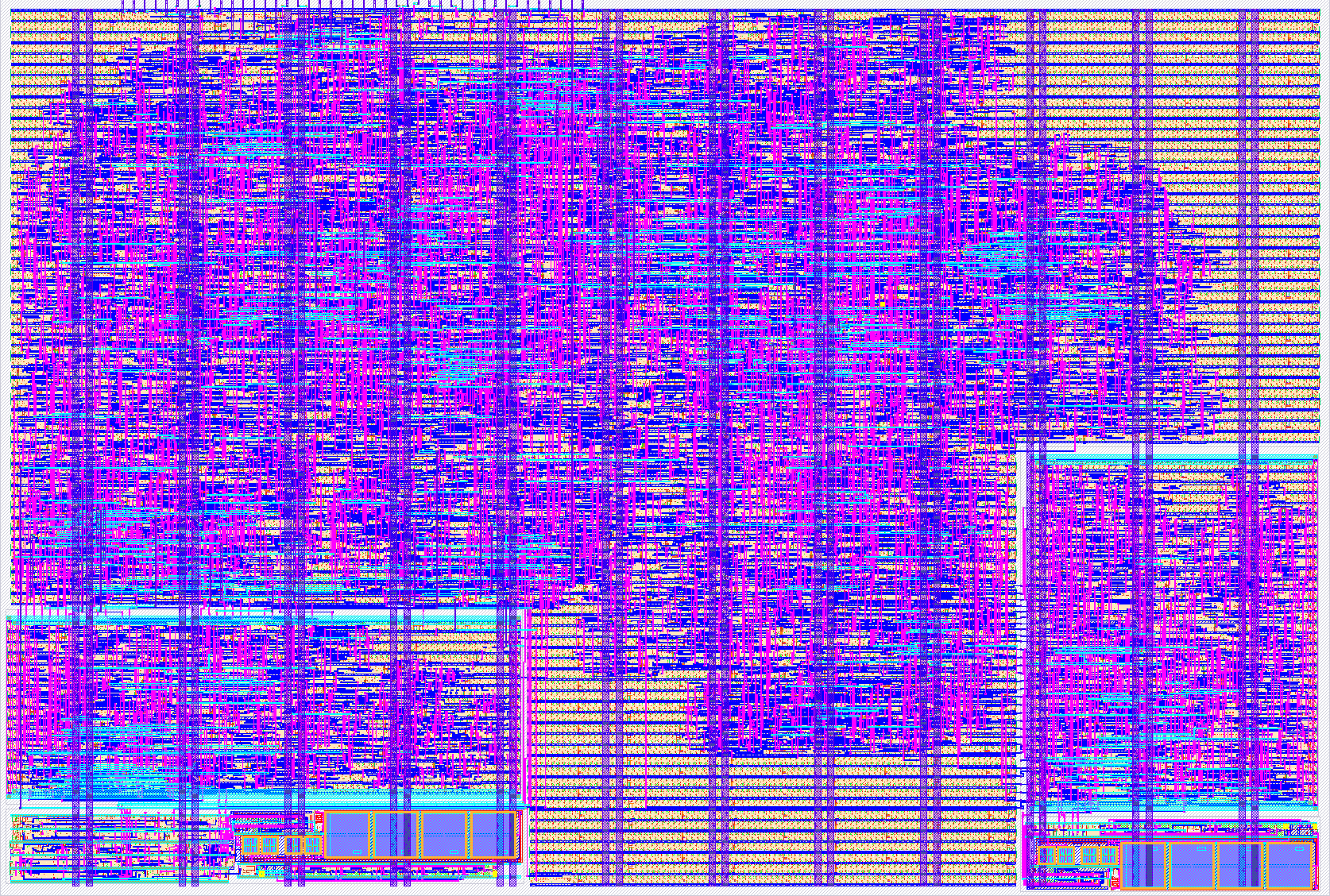
- Author: Paul Campbell
- Description: PLL/CDR/QuickBus test chip
- GitHub repository
- Open in 3D viewer
- Open in Tiny Tapeout Explorer
- Clock: 25 Hz
QuickBus
This Tiny Tapeout chip is a test chip for a QuickBus implementation, plus it's a second attempt at the Sky PLL taped out too quickly in Sky26b, this one should support a wider range of frequencies, hopefully up to 350MHz.
QuickBus is a prototype on-board chip to chip bus, think of it as SPI but up to 100 times faster - it's a 4-wire bus 2 bits each way with LVDS signalling. In this case the upstream and downstream are both in the same TT tile, no actual LVDS but full speed data tests, and tests for handling swapped LVDS pins.
How the PLL works
The PLL looks like this

On the left hand side are Sky HS logic blocks, they include a programmable clock scaler (a 4 bit down counter set by the COUNT_* pins), a reset logic that looks for clock stability and after detecting 16 good clocks asserts RESET_OUT_N, and a phase detector that compares the output of the clock scaler with a reference clock and drives the charge pump.
On the right are the analog blocks. Along the bottom is a variable frequency oscillator (VCO), 5 stages, Top left is the charge pump that drives the VCTRL output voltage into the oscillator. The 4 large square boxes to the right are capacitors charged from VCTRL through a long poly resistor that snakes the width of the block. The 2 small square boxes to the right are a smaller capacitor also on VCTRL.. The other 2 caps are decoupling caps for the charge pump.
Interface
The resulting block is intended to be a drop in to Sky TT projects, Its interface is very simple, inputs are:
- COUNT_3-COUNT_0 - these scale the reference clock by N-1 (so a value of 1 means 2 times, a value of 7 means 8 times) for example with a value of 7 and a 25MHz reference clock the PLL should generate 200MHz
- REFCLK - this is the input reference clock, this is intended to be connected to the Tiny Tapeout tile clock input. If you want more flexibility in generated frequencies you can divide down to a lower frequency, the phase detector only looks at the rising edge of the reference clock so it doesn't need to be a square wave (jitter added to the reference clock is reflected in jitter in the output clock).
- RESET_N - this an async reset, it can (should) be applied before the PLL starts. The PLL starts when RESET_N is released. It is intended to be connected directly to the Tiny Tapeout rst_n pin.
Outputs are:
- CLK - the resulting clock - at reset this in undefined, some time after RESET_N is removed it will be active at the desired frequency (COUNT+1)*f(REFCLK) (it's your responsibility to choose frequencies that the PLL can actually generate - roughly 50-300MHz, outside that range the results are undefined). Note in the rush to tape out the VCO range may have shifted up, 50MHa may not lock well - we'll see, that's what test tapeouts are for.
- RESET_OUT_N - this is a synchronous signal (wrt CLK) that is asserted by RESET_N until the clock is fairly stable - it's intended use is to hold a design in reset until the clock is stable, through the period when it might be thrashing around as the VCO starts up - your design should ignore the Tiny Tapeout rst_n and use this signal - note this signal is generated internally, your design might have a deep clock tree, it may be useful to run this through a flop before you use it to meet setup/hold. This signal is asserted by RESET_N and cleared when the clock becomes stable enough to use, it is not asserted again until RESET_N is asserted. This signal is cleared BEFORE the clock is completely stable (we'll characterize this with spice later), clock freq may go slightly higher that desired (a few percent) as it settles.
With the reference clock set to 25MHz these frequencies should be possible, anything after ~300MHz may not be real (out of the range of the VCO)
| COUNT | multiplier | CLK Freq |
|---|---|---|
| 0001 | 2 | 50MHz |
| 0010 | 3 | 75MHz |
| 0011 | 4 | 100MHz |
| 0100 | 5 | 125MHz |
| 0101 | 6 | 150MHz |
| 0110 | 7 | 175MHz |
| 0111 | 8 | 200MHz |
| 1000 | 9 | 225MHz |
| 1001 | 10 | 250MHz |
| 1010 | 11 | 275MHz |
| 1011 | 12 | 300MHz |
| 1100 | 13 | 325MHz* |
| 1101 | 14 | 350MHz* |
| 1110 | 15 | 375MHz* |
With a divides by 2 reference clock set to 12.5MHz these frequencies should be possible, number under 50MHz may be out of the range of the VCO)
| COUNT | multiplier | CLK Freq |
|---|---|---|
| 0001 | 2 | 25MHz* |
| 0010 | 3 | 37.5MHz* |
| 0011 | 4 | 50MHz |
| 0100 | 5 | 62.5MHz |
| 0101 | 6 | 75MHz |
| 0110 | 7 | 87.5MHz |
| 0111 | 8 | 100MHz |
| 1000 | 9 | 112.5MHz |
| 1001 | 10 | 125MHz |
| 1010 | 11 | 137.5MHz |
| 1011 | 12 | 150MHz |
| 1100 | 13 | 162.5MHz |
| 1101 | 14 | 175MHz |
| 1110 | 15 | 187.5MHz |
| 1111 | 15 | 200MHz |
QuickBus
Basic QuickBus looks like this
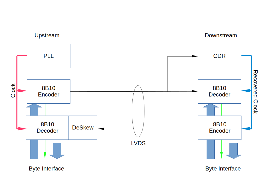
A QuickBus connects two chips over LVDS, it has an upstream chip and a downstream chip, if you want to compare it with SPI Upstream is 'M' and Downstream is 'S'. Upstream is in charge, Downstream responds.
Upstream has a PLL it sets the frequency for both sides, data is sent at all times even when idle, on the Downstream side is a Clock Data Recovery unit (essentially a PLL locked to the incoming data stream) downstream runs on the recovered clock (essentially the PLL's clock with some jitter and an arbitrary delay).
Data is sent/received using the standard 8b10 NRZ encoding - this sends 8 bits of data and a handful of framing symbols in 10 bits of on-wire data with a guaranteed number of edges to keep the CDR running. 8B10 has some minor error detection facilities, these are reported to the next layer up.
Data sent from Downstream to Upstream is sent with the Recovered Clock and received with the PLL clock, these are the same frequency clock - with a bit of jitter and an arbitrary delay (might be several bit times) - the Deskew is a variable length delay line and a phase detector that deals with the subbit-delay (and some jitter) followed by a variable length shift register to align the incoming symbols with outgoing ones.
On both sides a byte clock is generated (intended to be used by all the logic below the) this is the green arrows showed on the diagram above it is 1/10 the frequency of the PLL, both sides have the same clock, they have an arbitrary phase relationship.
The "Byte interface" is actually 9 bits, 8 data 'D' bits and a 'K' bit, if K is 0 the data is normal data, if it's a 1 then it's one of the standard 8b10 framing symbols, on reception K==1 and D==00 means an error.
Sitting above the bit framer and clock management is a management unit:
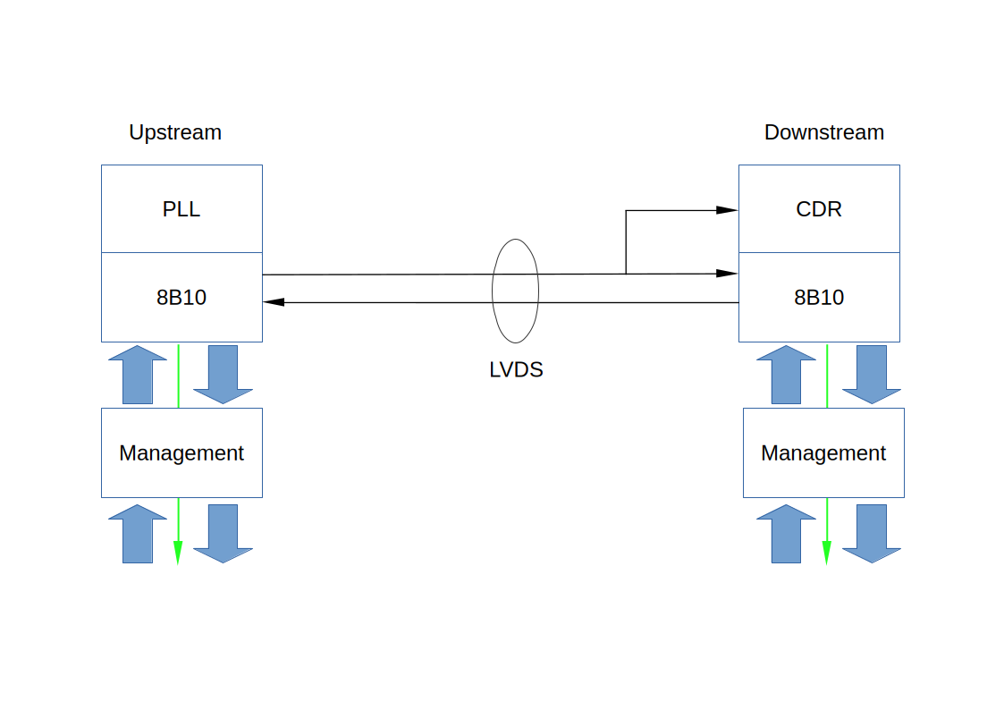
The management unit handles link startup, frequency negotiation, bus driver optimization and reversing miswired buses. It also handles error recovery, and (eventually) hot staging. When not in use it steps out of the way of the next level protocols.
The byte level interface is the same on both sides, it looks like:
System:
- CLK - 1/10 the PLL clock
- MGMT_OK - the link is up, you can now transmit - hen MGMT_OK is 0 RCV_READY will not be asserted and transmit requests will be ignored
Outgoing (outputs):
- XMT_D[7:0] - outgoing data
- XMT_K - outgoing symbol
- XMT_READY - data is sent when this is asserted, if not set an IDLE symbol is sent, IDLEs are swallowed by the remote receiver
Incoming (inputs):
- RCV_D[7:0] - incoming data
- RCV_K - incoming symbol
- RCV_READY - data is ready when this is asserted, there is no flow control so you must do something with the data or drop it
- RCV_ALIGN - this is set when EIE/END/EDB symbols are received or an error is detected - it is optional and is intended for systems where a fifo is used where the read port is multiple bytes wide
TBD - an upper level protocol for register/memory access (similar to existing SPI systems).
Multidrop
(may or may not get this in to TT this time)
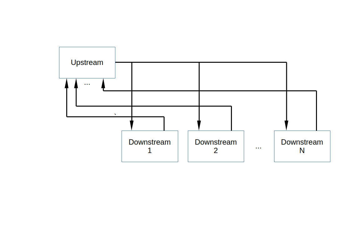
The basic idea here is that one Upstream node could talk to multiple Downstream nodes, sharing a single downstream data pair but each with a unique upstream pair for responses, Upstream chooses a PLL frequency that all devices can talk (and the wiring will handle). This means the Upstream needs N+1 pairs to talk to N devices while Downstream devices continue to need 2 pairs.
Implementation
This is a 2x2 TT tile.
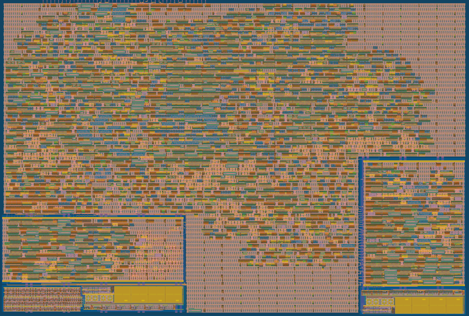
The Upstream side consists of two macros (lower left hand side), the PLL mentioned above and a standard cell macro called "deskew" which contains all the logic that has to run at the full speed clock (2-300MHz).
Deskew is sized to be the same width as the PLL and sits above it. Deskew contains the 1/10 clock generator and the output shift register, it also contains a variable length delay chain (lots of buffers and a mux tree) and a bang-bang phase discriminator, this feed a variable length shift register to do symbol alignment to the 1/10 clock.
The Downstream side also contains 2 macros, a Clock Data Recovery unit which consists of the charge pump from the PLL along with a modified 4 stage VCO that generates a quadrature clock signal, (upside down in the above image) ....
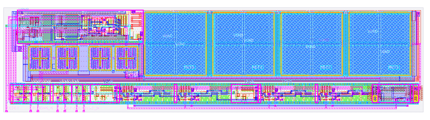 ....and a standard cell macro called "CDRS" that contains logic to sync to the incoming frequency and a bang-bang phase detector for station keeping, it also contains the high freq portion of the 8b10 encoders/decoders and generates the 1/10 clock synchronized to the symbols in the received bit stream.
The rest of the 8b10 logic (in the 1/10 clock domains), the management units and the logic to connect them to the external pins for test are synthesized into the remaining TT standard cell gates.
How to test
Interface
The Tiny Tapeout ui_in pins are sampled at the rising edge of rst_n. bits [7:6] determine the test mode:
- 0: PLL test - in this mode we just test the PLL - uii_in[3:0] are fed directly to the PLL and I/O mode 0 gives you access to the PLL's output
- 1: QuickBus simple - both upstream and downstream are connected to the I/O modes of the TT interface
- 2: QuickBus data - downstream generates a data stream
- 3: QuickBus registers - downstream has a simple register file
In the last three mode the lower 6 bits of ui_in are used for:
- 5: injects errors into the serial data streams depending on the I/O prog values
- 4: inverts the pins on the upstream->downstream link
- 3: injects errors on 300MHz streams
- 2:0 chooses the freq mask used for upstream
- 0: 100MHz
- 1: 100MHz
- 2: 100, 200MHz
- 3: 100, 200, 300MHz
- 4: 50, 100, 150, 200, 300MHz
- 5: 50, 100, 150, 200, 300, 500MHz
- 6: 50MHz
- 7: undefined
The top 2 pins of uio_in[7:6] choose the I/O mode, they can be changed on the fly once the system is running:
I/O mode 0:
- uo_out[7] - pll_clk
- uo_out[5] - upstream 1/10 clk
- uo_out[4] - downstream 1/10 clk
- uo_out[3:0] - counter clocked by pll_clk
- uio_out[5] - upstream 1/10 clk
- uio_out[4] - downstream 1/10 clk
- uio_out[3] - down_mgmt_ok - downstream link management is done
- uio_out[2] - up_mgmt_ok - upstream link management is done
- uio_out[1] - down_reset_n - downstream generated reset
- uio_out[0] - up_reset_n - upstream generated reset
I/O mode 1:
- in - downstream
- out - upstream
I/O mode 2:
- in - upstream
- out - downstream
I/O mode 3:
- in - upstream
- out - upstream
For the last 3 modes:
- uo_out - data out
- ui_in - data in
- uio_in[0] - k in
- uio_out[1] - k out
- uio_out[2] - in data ready
- uio_in[3] - out ready (see below)
- uio_out[4] - downstream clock
- uio_out[5] - upstream clock
Out ready is used to signal that new data is available, it's signaled by uio_in[5] being inverted from its previous state (so that it can be done manually from the TT test board)
simple test of PLL
Drive ui_in with 8'n0000_0001 (2 times freq), Set the TT clock to 25MHz. Assert reset, uo_out[1] should go low, clear reset, uo_out[1] should high. If we get this far the PLL is making a good clock. You can now look at the uo_out pins on a scope to check the freqs (should be 50MHz though that's at the tough lower end of the final VCO, 8'n0000_0010 will give you 75MHz, try looking at uo_out[3:2]which should be 1/2 and 1/4 the internal clock freq)
External hardware
a scope to look at the output signals
IO
| # | Input | Output | Bidirectional |
|---|---|---|---|
| 0 | din0 | dout0 | kin |
| 1 | din1 | dout1 | kout |
| 2 | din2 | dout2 | |
| 3 | din3 | dout3 | |
| 4 | din4 | dout4 | |
| 5 | din5 | dout5 | |
| 6 | din6 | dout6 | mode0 |
| 7 | din7 | dout7 | mode1 |