674 Zetterling SRAM
674 : Zetterling SRAM
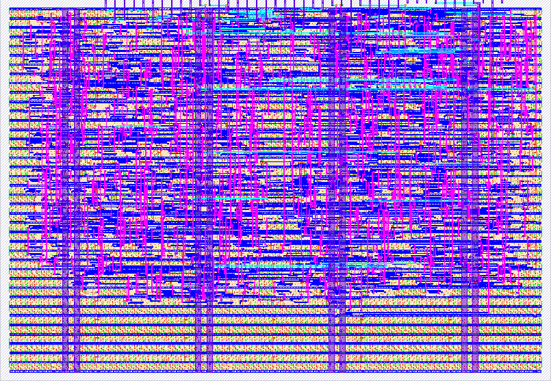
- Author: Carl-Mikael Zetterling
- Description: 128 bit SRAM
- GitHub repository
- Open in 3D viewer
- Open in Tiny Tapeout Explorer
- View in Wokwi
- Clock: 100000 Hz
Zetterling SRAM for Tiny Tapeout
SRAM Test using DFF or simpler registers (Wokwi version) Carl-Mikael Zetterling, 2026-07-18
Comment: I plan to replace this with a Verilog version by Sep 7
Online Workshop July 2026 SkyWater SKY130 TTSKY26c
RST_N: not used internally
CLK: used to store data
Uses the bi-directional pins for an 8 bit databus D0-D7 direction controlled by R/W pin
Inputs are used as follows: IN0: R/_W, reads if 0, writes if 1 IN1 - IN4: 4 pin Adress bus for 16 bytes of 8 bits
IN5: unused IN6: unused IN7: unused
OUT0 - OUT7: connected to 7-segment display or other OUT0: segment a OUT1: segment b OUT2: segment c OUT3: segment d OUT4: segment e OUT5: segment f OUT6: segment g OUT7: segment DP
How it works
The 3 address bits control a decoder to activate one row of DFFs The MUX at the DFF either feeds back Q, or the new Data Inputs The Q of the DFF goes to a Multiplexer reusing the Adress decoder and adding a 4 input OR gate made from 2-input ORs
How to test
Connect the address and data pins, select R/W = 1 and clock to write Connect address pins and LEDs to Data, select R/W = 0 to read (no clock)
External hardware
The 7 segment display or other LEDs can be used to monitor the outputs. For the bidirectional pins a bidirectional Tristate buffer and LEDs may be needed.
IO
| # | Input | Output | Bidirectional |
|---|---|---|---|
| 0 | RW | a | D0 |
| 1 | A0 | b | D1 |
| 2 | A1 | c | D2 |
| 3 | A2 | d | D3 |
| 4 | A3 | e | D4 |
| 5 | f | D5 | |
| 6 | g | D6 | |
| 7 | DP | D7 |