514 Oscillating Bones
514 : Oscillating Bones
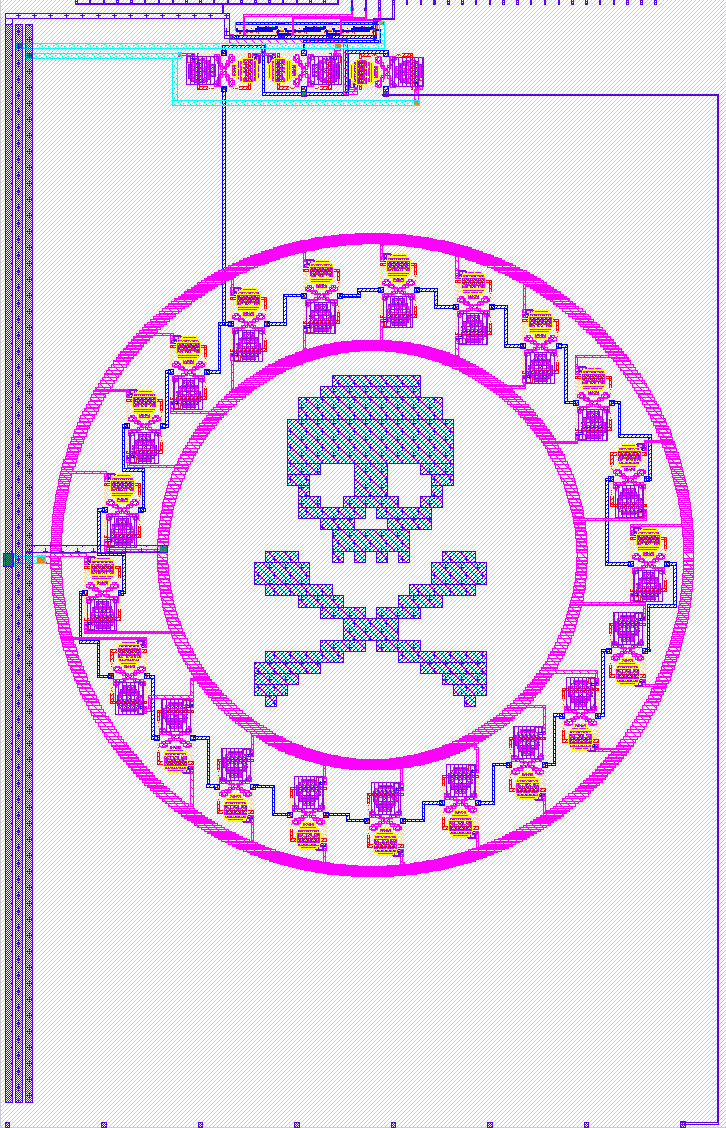
- Author: Uri Shaked
- Description: A stylish ring oscillator built from SkullFET transistors
- GitHub repository
- Open in 3D viewer
- Open in Tiny Tapeout Explorer
- Clock: 0 Hz
How it works
A simple yet stylish ring oscillator that uses a chain of 21 SkullFET inverters to generate a square wave. The ring runs from VAPWR, and its output fans out through a buffer into two independent branches:
ring (21 SkullFET inverters, VAPWR)
  |
  +-- SkullFET buffer (VAPWR)
        |
        +-- level shifter (VDPWR) --> uo_out[0] --> /2 /4 /8 --> uo_out[1..3]
        |
        `-- pad driver (VAPWR) -----> ua[0]
The buffer matters: it keeps the divider chain's input on an internal node, so the digital outputs work no matter what is connected to the analog pin.
Measured on silicon (ttsky25b), the ring runs at 178-180 MHz. Simulation of the extracted layout gives ~170 MHz.
| Pin | Signal | Frequency | Observable? |
|---|---|---|---|
| uo_out[0] | osc_out | ~180 MHz | Most likely no |
| uo_out[1] | osc_div_2 | ~90 MHz | Probably no |
| uo_out[2] | osc_div_4 | ~45 MHz | Marginal |
| uo_out[3] | osc_div_8 | ~22 MHz | Yes |
| ua[0] | osc_out_3v3 | ~180 MHz | Small signal only |
How to test
Use osc_div_8 on uo_out[3]. Connect a scope or logic analyzer and measure the period; multiply by 8 to get the ring frequency. The Tiny Tapeout GPIOs top out around 33 MHz, so osc_out, osc_div_2 and osc_div_4 are too fast to come out cleanly — expect them to look distorted or static.
About ua[0]: this is a small-signal tap, not a square wave. Roughly a kilohm of on-chip routing plus the pad and mux capacitance low-pass the node well below the ring frequency — no driver that fits in this tile could swing it rail-to-rail at 180 MHz. Expect on the order of 100 mV peak-to-peak sitting around 0.6-0.8 V DC.
The amplitude depends on your probe, so treat it as a qualitative "it's oscillating" indicator rather than a calibrated output.
Layout
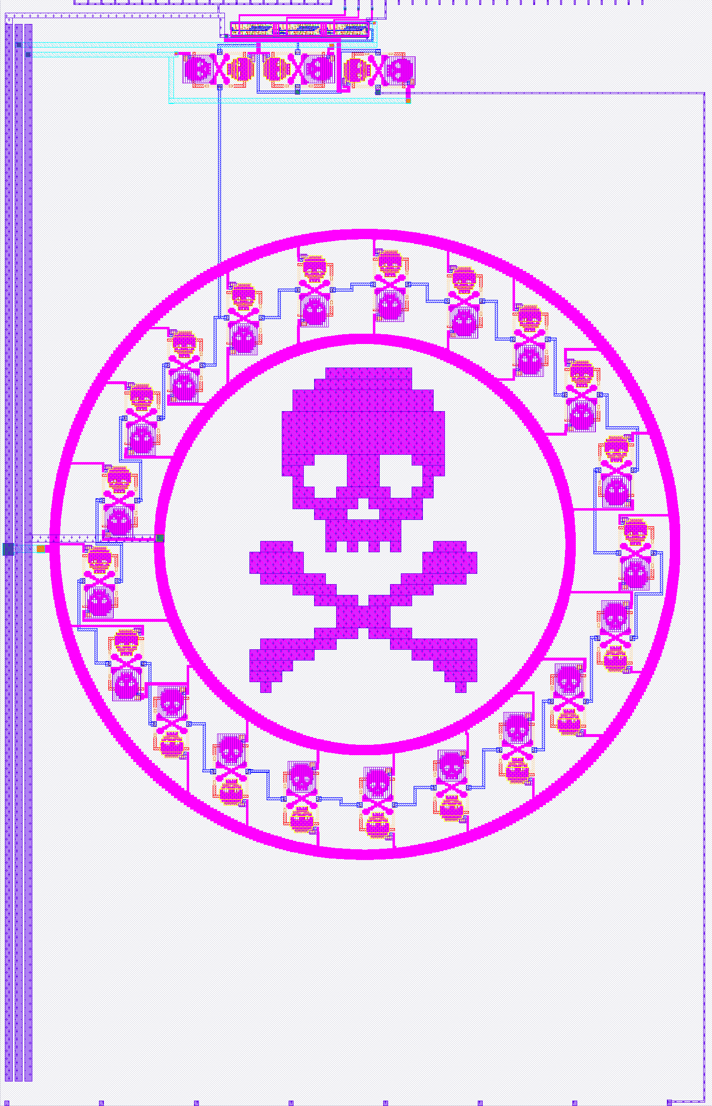
Twenty-one SkullFET inverters arranged in a ring around a big skull, with the buffer, level shifter, pad driver and divider chain along the top edge.
Simulation results
The following graph shows the output of the oscillator and the divided outputs. It was generated by running make -C sim and patiently waiting for the simulation to finish:
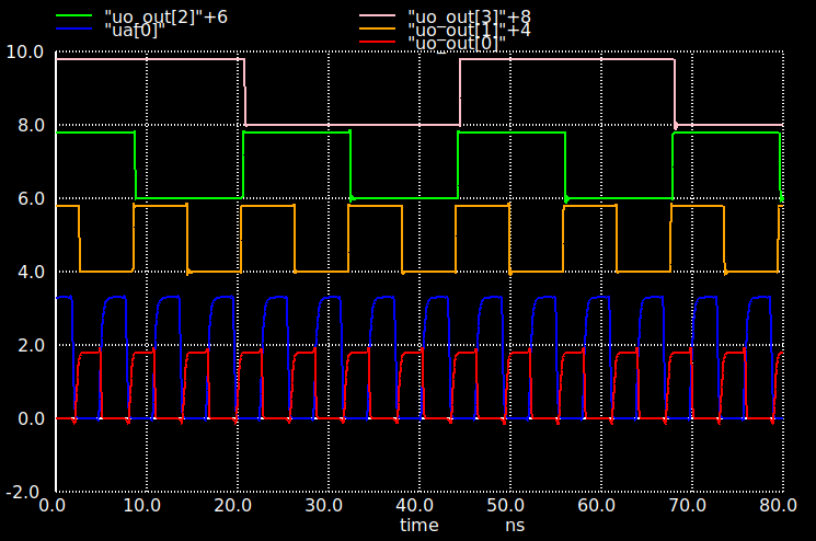
The outputs are shifted by 2 volts to make them easier to see in the graph. "uo_out[0]" is the main output of the oscillator, "ua[0]" is the analog output, and "uo_out[1]"/"uo_out[2]"/"uo_out[3]" are the divided outputs.
The testbench models the analog pad parasitics (series resistance plus pad capacitance on ua[0]); without them the simulation predicts a full-swing analog output that the silicon cannot produce.
IO
| # | Input | Output | Bidirectional |
|---|---|---|---|
| 0 | osc_out | ||
| 1 | osc_div_2 | ||
| 2 | osc_div_4 | ||
| 3 | osc_div_8 | ||
| 4 | |||
| 5 | |||
| 6 | |||
| 7 |
Analog pins
ua | PCB Pin | Internal index | Description |
|---|---|---|---|
| 0 | R | 10 | osc_out_3v3 |