490 SSF Capless LDO
490 : SSF Capless LDO
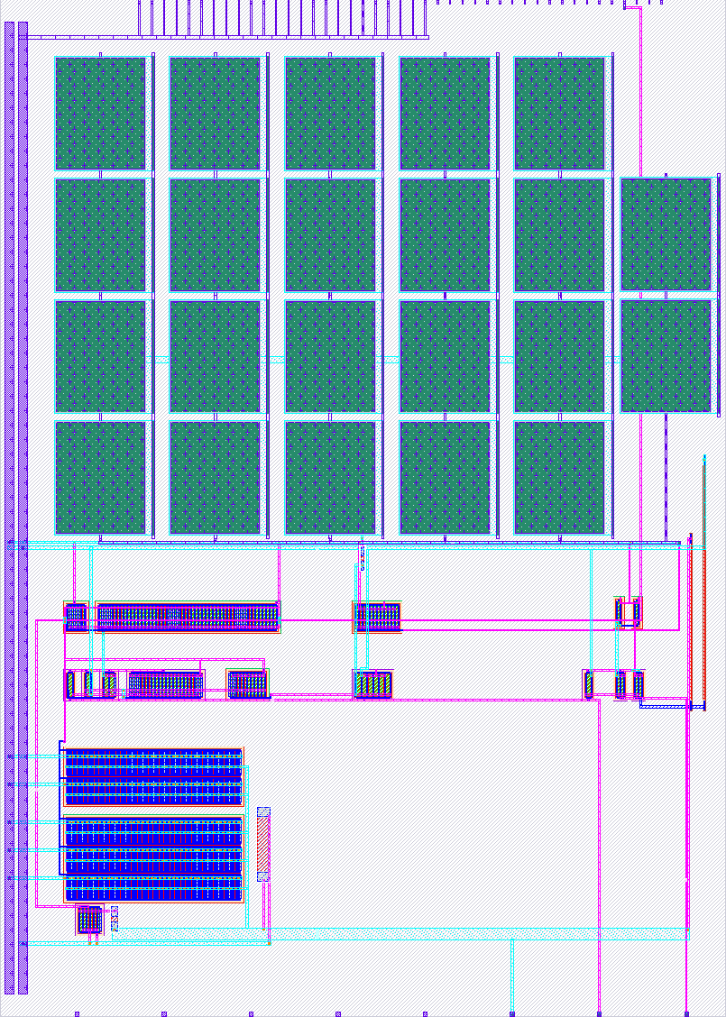
- Author: Billy Ouyang
- Description: 1.5V capless LDO: two-stage OTA + super source follower, on-chip 2.8mA demo load
- GitHub repository
- Open in 3D viewer
- Open in Tiny Tapeout Explorer
- Clock: 0 Hz
How it works
This tile is a fully analog low-dropout regulator: 16 FETs and 6 passives in SKY130A, no ideal sources, no digital gates.
Signal chain: a two-stage Miller-compensated OTA (NMOS input pair M1/M2 with PMOS mirror load M3/M4, second stage M7/M8) drives a super-source-follower buffer (Mb1, pfet_01v8_lvt in its own n-well), which drives the gate of a 2000 µm / 0.15 µm PMOS pass device. The pass FET is implemented as two parallel guard-ringed segments (Mp1 = 1200 µm, Mp2 = 800 µm) so that every point of the array sits within 15 µm of a well tap, satisfying the SKY130 latch-up rule LU.3. The output regulates to 1.5 V from the 1.8 V analog supply. The regulator is capless: compensation is fully internal (Miller + RZ), so no external output capacitor is required.
Feedback: an on-chip high-res poly divider (Rf1 = 0.35/35, Rf2 = 0.35/52.5 — exact 2:3 ratio) senses vldo and returns vfb = 0.6 × vldo to the error amplifier, compared against the external 0.9 V reference.
Compensation: 22 parallel MiM capacitors (cap_mim_m3_1) in series with a zero-cancelling poly resistor RZ (0.69/1.2) across the second stage.
Biasing: a single external 10 µA reference into a diode-connected NMOS (M6) is mirrored on-chip (Mb3–Mb6) into all internal branches, including the ~200 µA source feeding the follower stage. No other external bias is needed.
Load-step demo: driving ui_in[0] high turns on an on-chip switch (Msw, 30/0.5 nf6) in series with a 568 Ω poly resistor, stepping the load to roughly 2.8 mA so the transient response can be observed with no external load hardware.
Measured results (ngspice-46, sky130A models)
| Metric | Pre-layout (schematic) | Post-layout (C-extracted) |
|---|---|---|
| Phase margin, tt 27 °C | 63.1° | 59.6° |
| Phase margin, ss 125 °C | 55.4° | 51.8° |
| Phase margin, ff −40 °C | 73.7° | 70.7° |
| Unity-gain frequency (tt) | 2.19 MHz | 2.04 MHz |
| DC loop gain (tt) | 84.2 dB | 84.8 dB |
| Load-step droop (0.1 → ~2.8 mA) | −308 mV | −328 mV |
| Regulation point | 1.500 V | 1.5008 V (light and heavy load) |
| Dropout (pre-layout) | 14.8 mV @ 1.1 mA | — |
All corners clear the ≥45° stability floor with ≥6.8° to spare; the layout parasitic cost is a uniform 3.0–3.6° of phase margin across corners. Droop is quoted from a 0.1 mA bench baseline; with only the µA-scale divider load the dip is slightly deeper. The layout is DRC-clean — Tiny Tapeout precheck: 15/15 checks green — and LVS-clean (netgen: Circuits match uniquely). Bode and load-step plots are shown in the repository README; the full set lives in sim/.
How to test
- Power the board normally (VDPWR = 1.8 V analog supply).
- Apply 0.9 V to
ua[0](reference input, high-impedance). - Feed 10 µA into
ua[1]— this pin looks into a diode-connected NMOS sitting at ~0.7 V, so a ≈110 kΩ resistor from the 1.8 V rail works as a simple current source. - Observe 1.5 V on
ua[2](regulated output / sense). No output capacitor is needed; transient figures assume ~100 pF of board/probe parasitics on this node. - Toggle
ui_in[0]high to engage the on-chip switched load; a scope onua[2]shows a ~0.33 V droop with full recovery to 1.5 V. - Leave
ua[3..7]unconnected. All digital outputs of the tile are tied to ground internally.
External hardware
- 0.9 V reference for
ua[0](resistor divider or DAC) - ≈110 kΩ resistor from 1.8 V to
ua[1](10 µA bias) - Oscilloscope or DMM on
ua[2](no output capacitor required)
IO
| # | Input | Output | Bidirectional |
|---|---|---|---|
| 0 | load_en (on-chip 3mA demo load enable) | ||
| 1 | |||
| 2 | |||
| 3 | |||
| 4 | |||
| 5 | |||
| 6 | |||
| 7 |
Analog pins
ua | PCB Pin | Internal index | Description |
|---|---|---|---|
| 0 | D | 1 | vref (0.9V reference input) |
| 1 | G | 3 | ib0 (10uA bias current input) |
| 2 | F | 2 | vldo (LDO output sense) |