488 Continuous-Time Sigma-Delta ADC (1st order)
488 : Continuous-Time Sigma-Delta ADC (1st order)
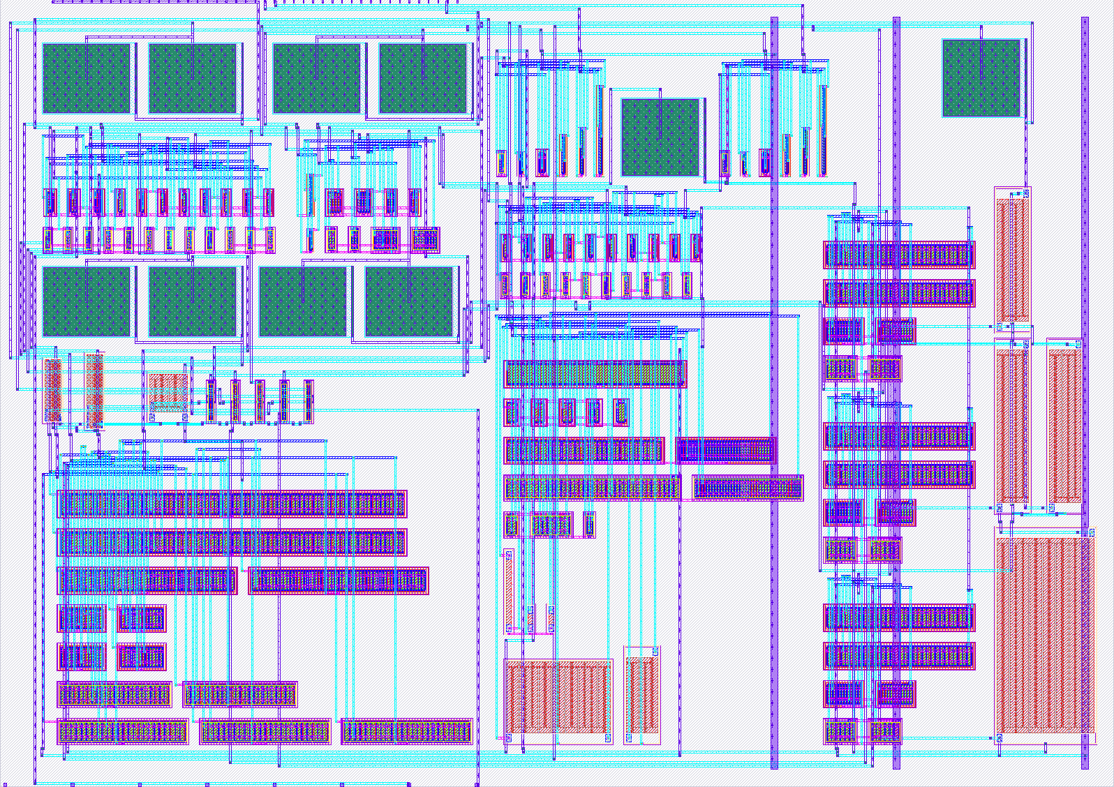
- Author: Paul Thomas
- Description: 1st-order continuous-time sigma-delta modulator ADC: active-RC integrator, StrongARM comparator, RZ resistive DAC
- GitHub repository
- Open in 3D viewer
- Open in Tiny Tapeout Explorer
- Clock: 50000000 Hz
How it works
A first-order continuous-time sigma-delta modulator analog-to-digital converter on the 3.3 V analog supply: an active-RC integrator (folded cascode operational transconductance amplifier), a StrongARM comparator with a retiming flip-flop, and a return-to-zero resistive feedback DAC. The 50 MHz bitstream is decimated off-chip two ways at once - a fast path (~1 MHz bandwidth, ≥6 ENOB, protection/trip use) and a precision path (~100 kHz, 10+ ENOB, measurement use).
The full design story - every architecture decision with its supporting data, the tiered verification methodology, and continuously-rebuilt simulation results - lives in the design repository and its generated design document:
- Design repo: https://gitlab.com/pthomas1/sigma-delta
- Living design document (CI-generated): see the GitLab Pages site of the design repo
Pinout: ua[0] = VIN (0-3.3 V about the 1.65 V mid-scale, through the on-chip 132k input resistor), ua[1] = integrator monitor (debug, high-impedance), uo[0]/uo[1] = Q/QB bitstream (1.8 V, capture synchronously), clk = 50 MHz.
Status: work in progress toward the shuttle deadline. The current GDS contains the verified OTA macro (DRC-clean, LVS-clean, parasitic- extracted and re-simulated); comparator, retimer, references, bias and top-level routing land next, from the same generated-and-verified flow.
How to test
Drive VIN (ua[0]) with a signal in the 0-3.3 V range, clock at 50 MHz, and decimate the Q/QB bitstream (uo[0]/uo[1]) with a sinc or CIC filter (an FPGA with a differential-capable input is the reference receiver).
External hardware
Low-jitter 50 MHz clock source; FPGA or logic analyzer to capture the bitstream.
IO
| # | Input | Output | Bidirectional |
|---|---|---|---|
| 0 | Q - modulator bitstream (1.8 V domain, retimed) | ||
| 1 | QB - complementary bitstream (pseudo-LVDS pair with uo[0]) | ||
| 2 | |||
| 3 | |||
| 4 | |||
| 5 | |||
| 6 | |||
| 7 |
Analog pins
ua | PCB Pin | Internal index | Description |
|---|---|---|---|
| 0 | G | 3 | VIN - analog input, 0-3.3 V around the 1.65 V mid-scale (through the on-chip 132k input resistor) |
| 1 | F | 2 | INT - integrator output monitor (OTA output, high impedance) |