271 Diff-In-Diff-Out-OpAmp
271 : Diff-In-Diff-Out-OpAmp
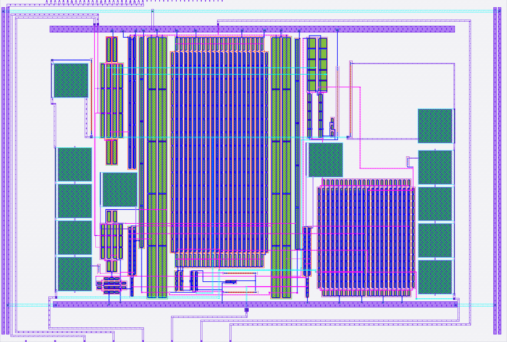
- Author: Bartosz Makowski
- Description: Fully-differential Class-AB folded-cascode operational amplifier in SKY130A
- GitHub repository
- Open in 3D viewer
- Open in Tiny Tapeout Explorer
- Clock: 0 Hz
How it works
This project is a fully-differential Class-AB folded-cascode operational amplifier implemented as a full-custom analog layout in SKY130A, running from the 1.8 V digital supply (VDPWR).
Architecture:
- Input stage — complementary input pair (NMOS + PMOS) giving a common-mode input range close to both rails (0.1 V to 1.7 V with ≥ 97 dB open-loop gain).
- Folded cascode — provides the high open-loop gain (100 dB typical) without stacking devices, which matters at 1.8 V.
- Class-AB output stage — translinear bias loop lets the output deliver ~1 mA peak from a 394 µA quiescent current, so the amplifier drives a 1 kΩ differential load without slew limiting at audio frequencies.
- Common-mode feedback (CMFB) — regulates the output common-mode level. The error pair uses source degeneration (2 ×
res_high_po_0p35, L = 17, ≈ 19.3 kΩ), which was needed to keep the CM loop bandwidth below the differential GBW; without it the CM loop oscillated at 6.7 MHz. - On-chip bias generator — a resistor/diode reference generates the internal NMOS bias, so only two external bias voltages are required.
Measured performance (post-layout, parasitic-extracted, typical corner, 27 °C):
| Parameter | Value |
|---|---|
| Open-loop gain | 100.3 dB |
| Gain-bandwidth product | 9.34 MHz |
| Phase margin | 57° |
| CMRR (DC) | 141 dB |
| PSRR+ (DC) | 88 dB |
| Slew rate | ±3.37 V/µs |
| THD @ 1 kHz, 1 Vpp | 0.000029 % |
| Output swing (THD < 1 %) | 0.37 V to 1.76 V |
| Output common-mode | 1.06 V |
| Quiescent current | 394 µA |
| Power | 0.71 mW |
Across all five process corners the open-loop gain stays between 90 dB and 108 dB, and the CMFB loop is stable from −20 °C to 125 °C.
Known limitations:
- The output is not rail-to-rail. The usable swing is ±0.70 V around the output common-mode level, which is set by the CMFB reference rather than by the output devices. The input is rail-to-rail.
- Differential phase margin drops below 45° below 27 °C, and in the fast-NMOS/slow-PMOS corner at 27 °C it is 41°. This is a small-signal AC result — the large-signal step response stays smooth with no ringing even at the worst corner, so the amplifier remains usable, but stability margin is reduced at low temperature.
How to test
Supplies and bias
The amplifier needs two external bias voltages in addition to the 1.8 V supply:
| Pin | Apply |
|---|---|
ua[0] |
0.3 V (PMOS cascode bias, Vp) |
ua[2] |
1.5 V (Class-AB bias, Vn) |
These draw negligible current and can come from a resistive divider or a bench supply.
Basic functional check (closed loop, gain = −1)
Wire four 10 kΩ resistors in the standard fully-differential inverting configuration:
   Vin+ ──[10k]──┬── ua[5] (Vinp)
                 │
        [10k]────┘   ... to ua[1] (Voutm)

   Vin- ──[10k]──┬── ua[4] (Vinm)
                 │
        [10k]────┘   ... to ua[3] (Voutp)
Note the cross-coupling: the feedback resistor from ua[1] (Voutm) goes to ua[5] (Vinp), and the one from ua[3] (Voutp) goes to ua[4] (Vinm). Connecting them straight through gives positive feedback and the outputs will latch to the rails.
Add a 1 kΩ resistor between ua[3] and ua[1] as the differential load.
Drive the inputs with a 1 kHz differential sine, 1 Vpp (i.e. ±0.25 V on each input, in antiphase, centred on 0.9 V). You should see:
- a clean 1 Vpp differential sine at the output, in antiphase with the input
- closed-loop gain of about 0.995 (the 0.5 % error is the expected finite-loop-gain error at a 1 kΩ load)
- the output common-mode sitting at about 1.06 V and staying there
Open loop
Do not try to measure gain in open loop — with 100 dB of gain and a few millivolts of offset the outputs will sit at the rails. All measurements should be made in a closed-loop configuration.
External hardware
No PMOD or dedicated board is required. You need:
- two bias voltages: 0.3 V and 1.5 V (bench supply or resistive dividers)
- four 10 kΩ resistors for the feedback network, and one 1 kΩ load resistor
- a differential signal source, or a single-ended source with a transformer/inverter to generate the antiphase input
- an oscilloscope or audio analyser on the differential output
IO
| # | Input | Output | Bidirectional |
|---|---|---|---|
| 0 | |||
| 1 | |||
| 2 | |||
| 3 | |||
| 4 | |||
| 5 | |||
| 6 | |||
| 7 |
Analog pins
ua | PCB Pin | Internal index | Description |
|---|---|---|---|
| 0 | Q | 11 | Vp - PMOS cascode bias input, 0.3 V |
| 1 | W | 7 | Voutm - negative output |
| 2 | X | 6 | Vn - class-AB bias input, 1.5 V |
| 3 | R | 10 | Voutp - positive output |
| 4 | T | 9 | Vinm - inverting input |
| 5 | U | 8 | Vinp - non-inverting input |